FS61857-01 Просмотр технического описания (PDF) - AMI Semiconductor
Номер в каталоге
Компоненты Описание
производитель
FS61857-01 Datasheet PDF : 7 Pages
| |||
AMERICAN MICROSYSTEMS, INC.
FS61857-01
1:10 HSTL Zero-Delay Clock Buffer IC
November 2000
Advance Information
1.0 Features
• Generates one bank of ten differential 2.5V HSTL
clock outputs (YP0/YN0 to YP9/YN9) from one differ-
ential HSTL reference clock input
• Meets the JEDEC Standard PLL Clock Driver for
Registered DIMM Applications
• External feedback input (FBINP/FBINN) to synchro-
nize all clock outputs to the reference input
• Operating frequency 60MHz to 170MHz
• Tight tracking skew (spread-spectrum tolerant)
• Integrated 25Ω series damping resistors for driving
point-to-point loads
• Auto power-down mode if reference input frequency
drops below 20MHz
• Active-low power-down signal (PWRDWN#) tristates
all output drivers and disables the PLL
• Packaged in a 48-pin TSSOP
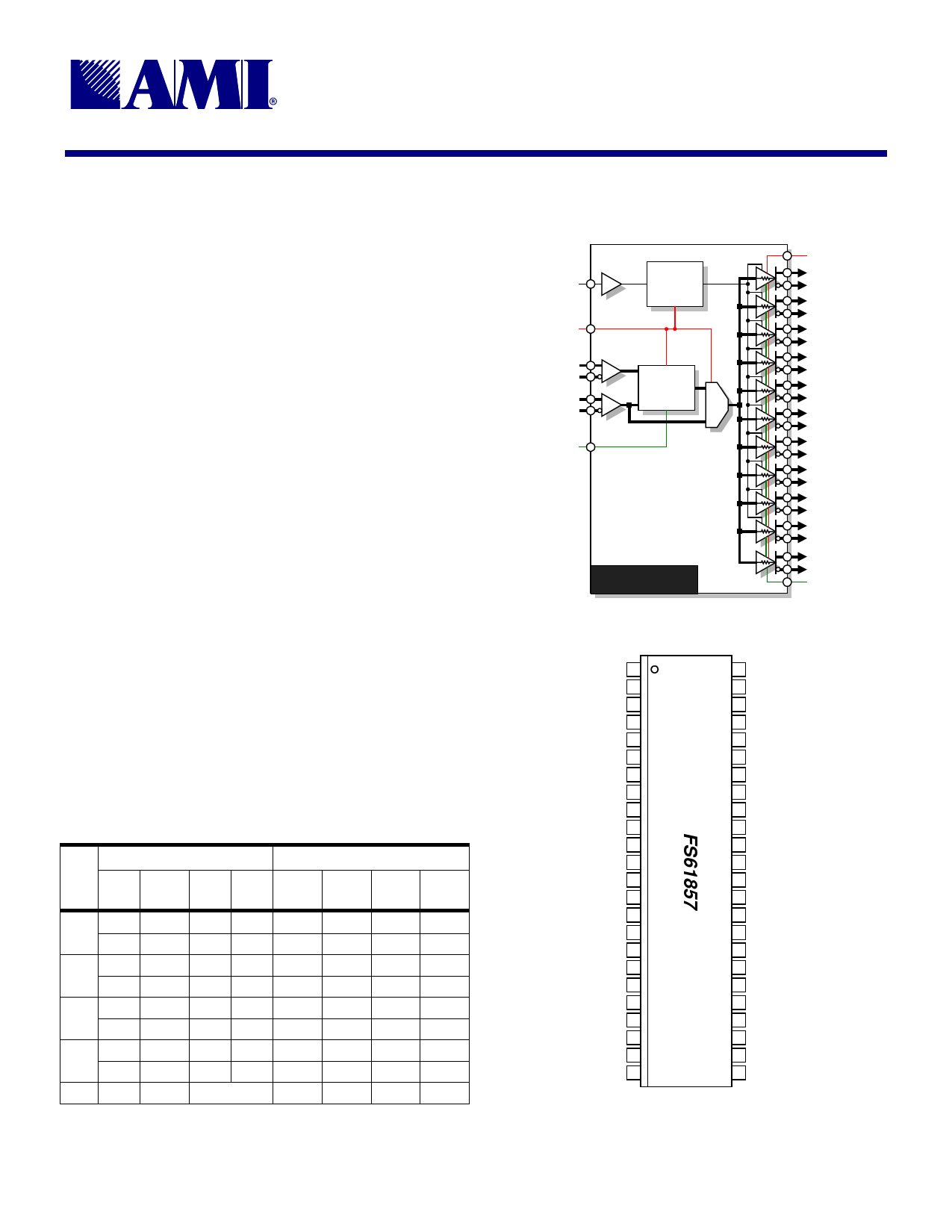
Figure 1: Block Diagram
PWRDWN#
AVDD
FBINP
FBINN
CKP
CKN
AGND
Power
Down
PLL
FS61857
VDD
YP0
YN0
YP1
YN1
YP2
YN2
YP3
YN3
YP4
YN4
YP5
YN5
YP6
YN6
YP7
YN7
YP8
YN8
YP9
YN9
FBOUTP
FBOUTN
GND
2.0 Description
The FS61857 is a low skew, low jitter CMOS zero-delay
phase-lock loop (PLL) clock buffer IC. Ten differential
buffered clock outputs are derived from an onboard open-
loop PLL. The PLL aligns the frequency and phase of all
output clock pairs to the differential reference input clock
CLKP/CLKN, including a feedback output clock pair that
feeds back to FBINP/FBINN to close the loop. The PLL
can be bypassed for test purposes by pulling AVDD to
ground.
Table 1: Function Table
INPUT
PLL
AVDD
PWR
DWN#
CKP
CKN
2.5V L
OFF
2.5V L
Zero- 2.5V
H
Delay 2.5V
H
GND L
OFF
GND L
PLL GND
H
Bypass GND
H
OFF -
-
L
H
H
L
L
H
H
L
L
H
H
L
L
H
H
L
<20MHz
YP0-
YP9
Z
Z
L
H
Z
Z
L
H
Z
OUTPUT
YN0- FBOUT FBOUT
YN9
P
N
Z
Z
Z
Z
Z
Z
H
L
H
L
H
L
Z
Z
Z
Z
Z
Z
H
L
H
L
H
L
Z
Z
Z
Figure 2: Pin Configuration
GND 1
YN0 2
YP0 3
VDD 4
YP1 5
YN1 6
GND 7
GND 8
YN2 9
YP2 10
VDD 11
VDD 12
CKP 13
CKN 14
VDD 15
AVDD 16
AGND 17
GND 18
YN3 19
YP3 20
VDD 21
YP4 22
YN4 23
GND 24
48 GND
47 YN5
46 YP5
45 VDD
44 YP6
43 YN6
42 GND
41 GND
40 YN7
39 YP7
38 VDD
37 PWRDWN#
36 FBINP
35 FBINN
34 VDD
33 FBOUTN
32 FBOUTP
31 GND
30 YN8
29 YP8
28 VDD
27 YP9
26 YN9
25 GND
ISO9001
QS9000
This document contains information on a preproduction product. Specifications and information herein are subject to change without notice.
11.14.00
Share Link: 