LM2594 Просмотр технического описания (PDF) - ON Semiconductor
Номер в каталоге
Компоненты Описание
производитель
LM2594 Datasheet PDF : 25 Pages
| |||
LM2594
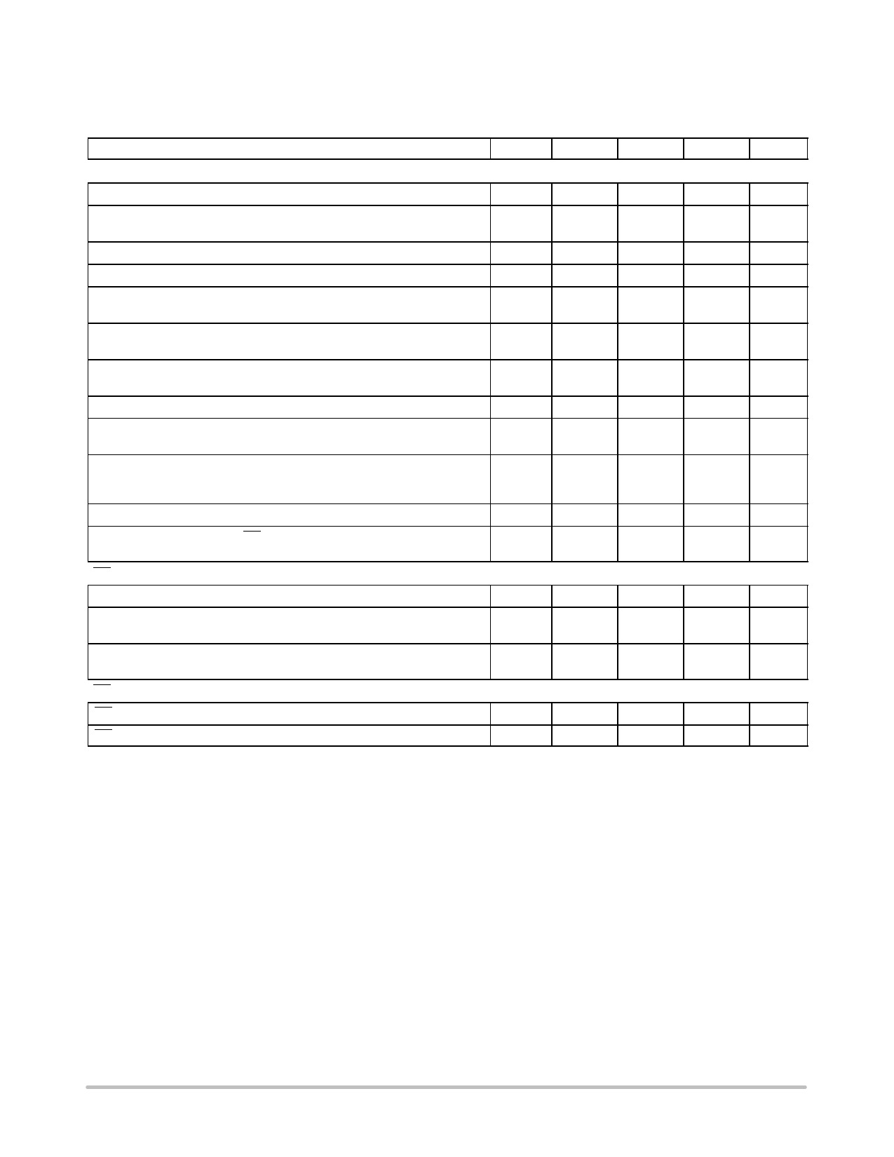
SYSTEM PARAMETERS
ELECTRICAL CHARACTERISTICS Specifications with standard type face are for TJ = 25°C, and those with boldface type apply
over full Operating Temperature Range −40°C to +125°C
Characteristics
Symbol
Min
Typ
Max
Unit
LM2594 (Note 1, Test Circuit Figure 16)
Feedback Voltage (Vin = 12 V, ILoad = 0.1 A, Vout = 5.0 V, )
VFB_nom
1.23
V
Feedback Voltage (8.0 V ≤ Vin ≤ 40 V, 0.1 A ≤ ILoad ≤ 0.5 A, Vout = 5.0 V)
VFB
1.193
1.18
1.267
V
1.28
Efficiency (Vin = 12 V, ILoad = 0.5 A, Vout = 5.0 V)
Characteristics
η
−
80
%
Symbol
Min
Typ
Max
Unit
Feedback Bias Current (Vout = 5.0 V)
Ib
25
100
nA
200
Oscillator Frequency (Note 2)
fosc
135
150
165
kHz
120
180
Saturation Voltage (Iout = 0.5 A, Notes 3 and 4)
Vsat
1.0
1.2
V
1.4
Max Duty Cycle “ON” (Note 4)
DC
95
%
Current Limit (Peak Current, Notes 3 and 4)
ICL
0.7
1.0
1.6
A
0.65
1.8
Output Leakage Current (Notes 5 and 6)
Output = 0 V
Output = −1.0 V
IL
mA
0.5
2.0
13
30
Quiescent Current (Note 5)
Standby Quiescent Current (ON/OFF Pin = 5.0 V (“OFF”))
(Note 6)
IQ
5.0
10
mA
Istby
50
200
mA
250
ON/OFF PIN LOGIC INPUT
Threshold Voltage
1.6
V
Vout = 0 V (Regulator OFF)
VIH
2.2
V
2.4
Vout = Nominal Output Voltage (Regulator ON)
VIL
1.0
V
0.8
ON/OFF Pin Input Current
ON/OFF Pin = 5.0 V (Regulator OFF)
IIH
−
15
30
mA
ON/OFF Pin = 0 V (regulator ON)
IIL
−
0.01
5.0
mA
1. External components such as the catch diode, inductor, input and output capacitors can affect switching regulator system performance.
When the LM2594 is used as shown in the Figure 16 test circuit, system performance will be as shown in system parameters section.
2. The oscillator frequency reduces to approximately 30 kHz in the event of an output short or an overload which causes the regulated output
voltage to drop approximately 40% from the nominal output voltage. This self protection feature lowers the average dissipation of the IC by
lowering the minimum duty cycle from 5% down to approximately 2%.
3. No diode, inductor or capacitor connected to output (Pin 8) sourcing the current.
4. Feedback (Pin 4) removed from output and connected to 0 V.
5. Feedback (Pin 4) removed from output and connected to +12 V to force the output transistor “off”.
6. Vin = 40 V.
http://onsemi.com
4
Share Link: 