TDA9210 Просмотр технического описания (PDF) - STMicroelectronics
Номер в каталоге
Компоненты Описание
производитель
TDA9210 Datasheet PDF : 19 Pages
| |||
TDA9210
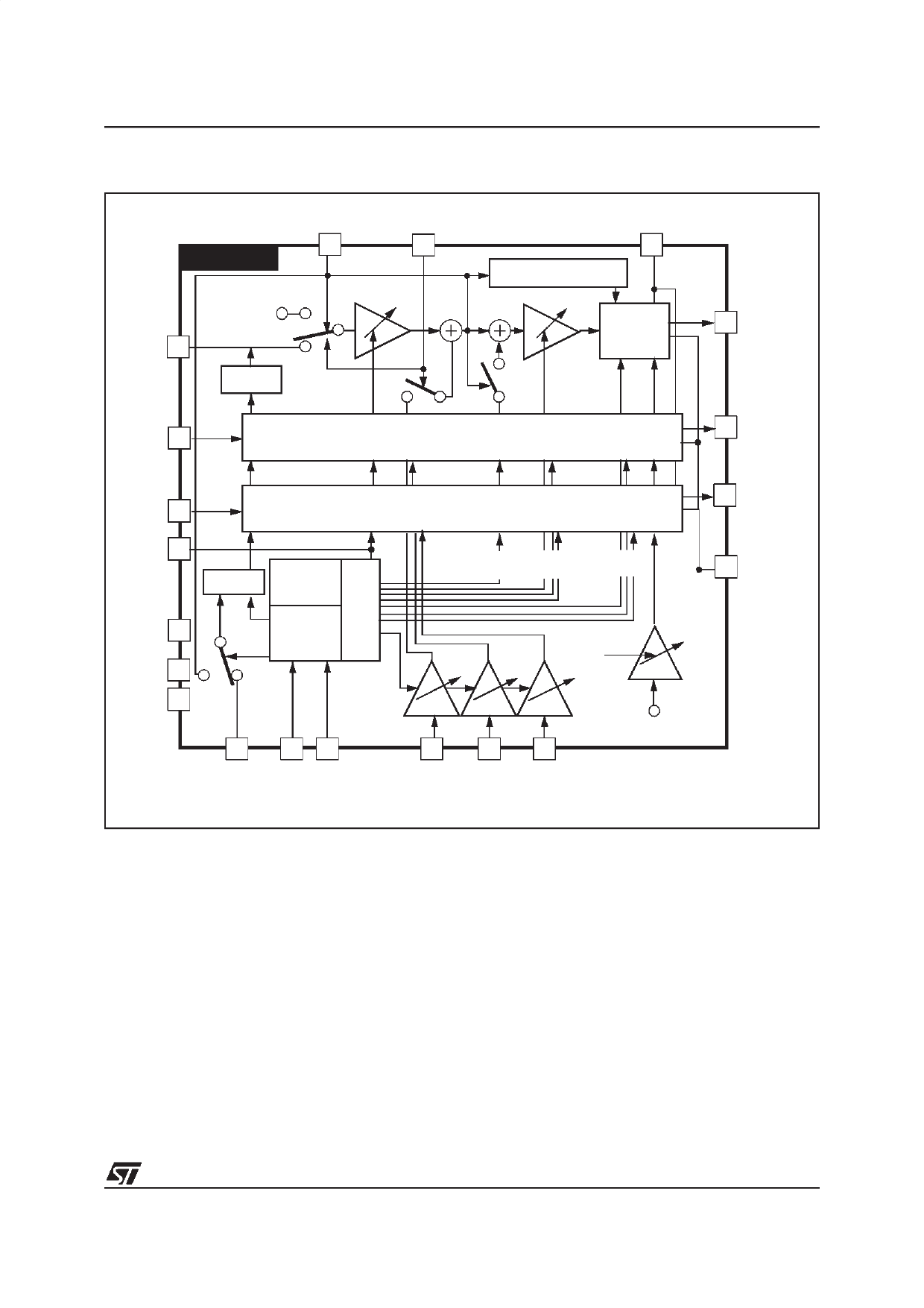
3 - BLOCK DIAGRAM
TDA9210
IN1 1
VREF
Clamp
BLK
FBLK
20
11
Contrast
Output Clamp Pulse
(OCL)
Drive
VCCP
17
Output
Stage
IN2 3
Green Channel
18 OUT1
16 OUT2
IN3 5
Blue Channel
14 OUT3
ABL 2
GNDL 4
GNDA 6
VCCA 7
Contrast/8bit
BPCP
Latches
I2C
D/A
Bus
Decoder
OSD
Cont.
4bits
Brightness Drive
8bits 3x8bits
Cut-off
8bits
15 GNDP
Output
DC Level
IC
4bits
VREF
19
13 12
HSYNC SDA SCL
or BPCP
8
9
10
OSD1 OSD2 OSD3
See Figure 8 for complete BPCP and OCL generation diagram
4 - FUNCTIONAL DESCRIPTION
4.1 - RGB Input
The three RGB inputs have to be supplied through
coupling capacitors (100 nF).
The maximum input peak-to-peak video amplitude
is 1 V.
The input stage includes a clamping function. The
clamp uses the input serial capacitor as a ”memo-
ry capacitor”.
To avoid a discharge of the serial capacitor during
the line (due to leakage current), the input voltage
is referenced to the ground.
The clamp is gated by an internally generated
”Back Porch Clamping Pulse” (BPCP). Register 8
allows to choose the way to generate this BPCP
(see Figure 1).
When bit 0 is set to 0, the BPCP is synchronized
on the trailing or leading edge of HSYNC (Pin 19)
(bit 1 = 0: trailing edge, bit 1 = 1: leading edge).
3/19
Share Link: 