NUF6105FC Просмотр технического описания (PDF) - ON Semiconductor
Номер в каталоге
Компоненты Описание
производитель
NUF6105FC Datasheet PDF : 6 Pages
| |||
NUF6105FC
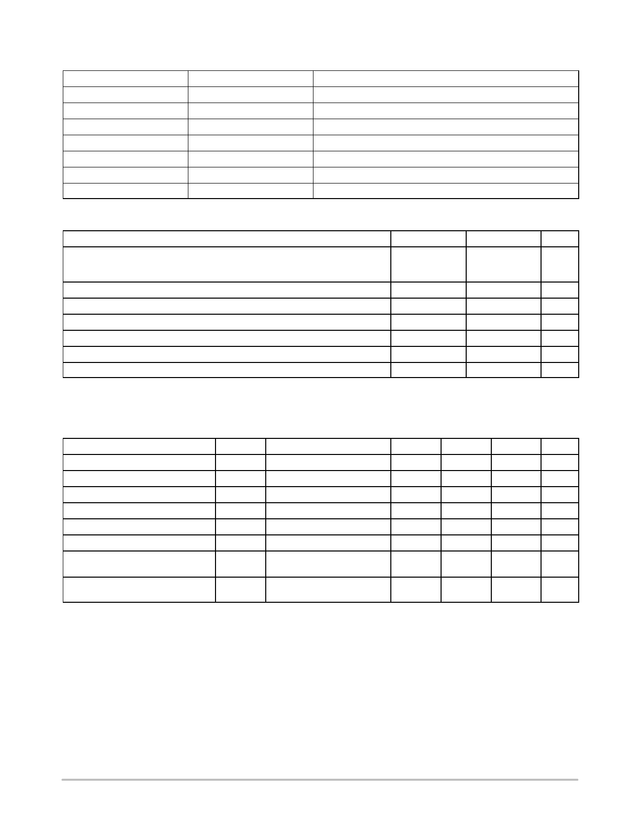
Table 1. FUNCTIONAL PIN DESCRIPTION
Filter
Device Pins
Filter 1
1 & 12
Filter 2
2 & 11
Filter 3
3 & 10
Filter 4
4&9
Filter 5
5&8
Filter 6
6&7
Ground Pad
GND
Filter + ESD Channel 1
Filter + ESD Channel 2
Filter + ESD Channel 3
Filter + ESD Channel 4
Filter + ESD Channel 5
Filter + ESD Channel 6
Ground
Description
MAXIMUM RATINGS
Parameter
Symbol
Value
Unit
ESD Discharge IEC61000−4−2
Contact Discharge
VPP
Machine Model
Human Body Model
30
kV
30
16
DC Power per Resistor
PR
100
mW
DC Power per Package
PT
600
mW
Junction Temperature
TJ
150
°C
Operating Temperature Range
TOP
−40 to 85
°C
Storage Temperature Range
TSTG
−55 to 150
°C
Maximum Lead Temperature for Soldering Purposes (1.8 in from case for 10 seconds)
TL
260
°C
Stresses exceeding Maximum Ratings may damage the device. Maximum Ratings are stress ratings only. Functional operation above the
Recommended Operating Conditions is not implied. Extended exposure to stresses above the Recommended Operating Conditions may affect
device reliability.
ELECTRICAL CHARACTERISTICS (TJ = 25°C unless otherwise noted)
Parameter
Symbol
Test Conditions
Min
Typ
Max
Unit
Maximum Reverse Working Voltage
VRWM
5.0
V
Breakdown Voltage
VBR
IR = 10 mA
6.0
7.0
8.0
V
Leakage Current
IR
VRWM = 3.3 V
100
nA
Resistance
RA
IR = 20 mA
80
100
120
W
Diode Capacitance
Cd
VR = 2.5 V, f = 1.0 MHz
27
pF
Line Capacitance
CL
VR = 2.5 V, f = 1.0 MHz
54
pF
3 dB Cut−Off Frequency (Note 1)
f3dB
Above this frequency,
100
appreciable attenuation occurs
MHz
6 dB Cut−Off Frequency (Note 1)
f6dB
Above this frequency,
180
appreciable attenuation occurs
MHz
1. 50 W source and 50 W load termination.
http://onsemi.com
2
Share Link: 