PM25LV020-33QCE Просмотр технического описания (PDF) - PMC-Sierra, Inc
Номер в каталоге
Компоненты Описание
производитель
PM25LV020-33QCE
PMC-Sierra, Inc

PM25LV020-33QCE Datasheet PDF : 32 Pages
| |||
PMC
Pm25LV010/020/040
REGISTERS (CONTINUED)
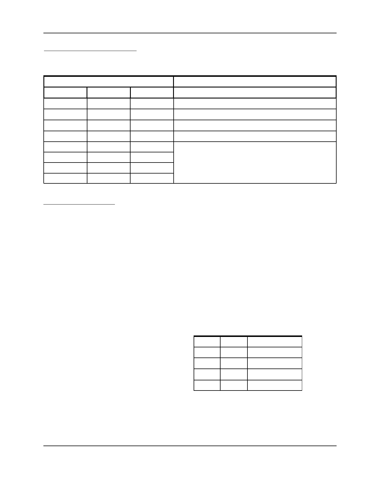
Table 6. Block Write Protect Bits for Pm25LV040
BP2
0
0
0
0
1
1
1
1
Status Register Bits
BP1
0
0
1
1
0
0
1
1
BP0
0
1
0
1
0
1
0
1
Protected Memory Area
4 Mbit
None
Upper eighth (Block 7): 070000h - 07FFFFh
Upper quarter (Block 6 and 7): 060000h - 07FFFFh
Upper half (Block 4 and 7): 040000h - 07FFFFh
All Blocks (Block 0 to 7):
000000h - 03FFFFh
PROTECTION MODE
The Pm25LV010/020/040 have two protection modes:
hardware write protection and software write protection
to prevent any irrelevant operation under a possible noisy
environment and protect the data integrity.
HARDWARE WRITE PROTECTION
The devices provide two hardware write protection
features:
a. When input any program, erase or write status regis-
ter instruction, the number of clock pulse will be
checked whether it is a multiple of eight before the
execution of such instruction. Any incomplete instruc-
tion command sequence will be ignored.
b. The devices feature a Write Protection (WP#) pin to
provide a hardware write protection method for BP2,
BP1,BP0 abd SRWD in the Status Register.
(1)When the WP# is pulled low (VIL), the Status
Register is write protected if the SRWD bit is enabled
(Refer to Table 7 for Hardware Write Protection on
Status Register). Hence part or whole memory area
can be write protected depends on the setting of BP2,
BP1 and BP0 bits.
(2) When the WP# is pulled high (V ), the Status
IH
Register is not protected, BP2,BP1,BP0 and SRWD
can be changed.
SOFTWARE WRITE PROTECTION
The Pm25LV010/020/040 also provide two software write
protection features:
a. Before the execution of any program, erase or write
status register instruction, the Write Enable Latch
(WEL) bit must be enabled by execution of the Write
Enable (WREN) instruction. If the WEL bit is not en-
abled first, the program, erase or write register in-
struction will be ignored.
b. The Block Protection (BP2, BP1, BP0) bits allow part
or whole memory area to be write protected.
Table 7. Hardware Write Protection on Status
Register
SRWD
0
1
0
1
WP#
Low
Low
High
High
Status Register
Writable
Protected
Writable
Writable
Programmable Microelectronics Corp.
9
Issue Date: July, 2005, Rev: 1.2
Share Link: