LT3574 Просмотр технического описания (PDF) - Linear Technology
Номер в каталоге
Компоненты Описание
производитель
LT3574 Datasheet PDF : 24 Pages
| |||
LT3574
Applications Information
Overdriving the BIAS Pin with a Third Winding
The LT3574 provides excellent output voltage regulation
without the need for an opto-coupler, or third winding, but
for some applications with higher input voltages (>20V),
it may be desirable to add an additional winding (often
called a third winding) to improve the system efficiency.
For proper operation of the LT3574, if a winding is used as
a supply for the BIAS pin, ensure that the BIAS pin voltage
is at least 3.15V and always less than the input voltage.
For a typical 24VIN application, overdriving the BIAS pin
will improve the efficiency gain 4% to 5%.
Loop Compensation
The LT3574 is compensated using an external resistor-
capacitor network on the VC pin. Typical values are in the
range of RC = 50k and CC = 1nF (see the numerous sche-
matics in the Typical Applications section for other possible
values). If too large of an RC value is used, the part will be
more susceptible to high frequency noise and jitter. If too
small of an RC value is used, the transient performance will
suffer. The value choice for CC is somewhat the inverse
of the RC choice: if too small a CC value is used, the loop
may be unstable, and if too large a CC value is used, the
transient performance will also suffer. Transient response
plays an important role for any DC/DC converter.
Design Example
The following example illustrates the converter design
process using LT3574.
Given the input voltage of 20V to 28V, the required output
is 5V, 0.5A.
VIN(MIN) = 20V, VIN(MAX) = 28V, VOUT = 5V, VF = 0.5V
and IOUT = 0.5A
1. Select the transformer turns ratio to accommodate
the output.
The output voltage is reflected to the primary side by a
factor of turns ratio N. The switch voltage stress VSW is
expressed as:
N = NP
NS
VSW(MAX) = VIN + N(VOUT + VF ) < 50V
or rearranged to:
N < 50 − VIN(MAX)
(VOUT + VF )
On the other hand, the primary-side current is multiplied by
the same factor of N. The converter output capability is:
IOUT(MAX)
=
0.8
•
(1−
D)
•
1
2
NIPK
D = N(VOUT + VF )
VIN + N(VOUT + VF )
The transformer turns ratio is selected such that the con-
verter has adequate current capability and a switch stress
below 50V. Table 6 shows the switch voltage stress and
output current capability at different transformer turns
ratio.
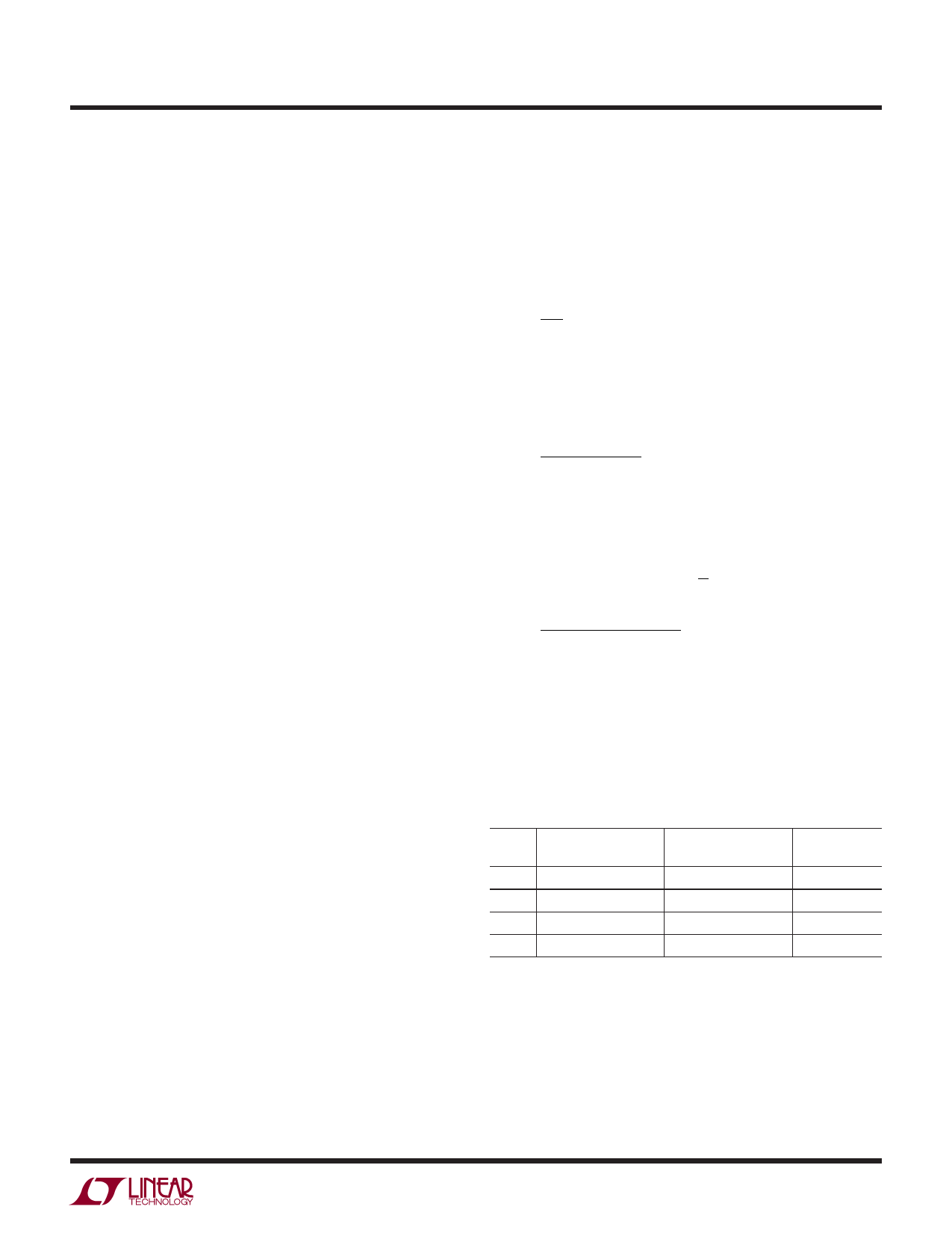
Table 6. Switch Voltage Stress and Output Current Capability vs
Turns Ratio
VSW(MAX) AT VIN(MAX) IOUT(MAX) AT VIN(MIN) DUTY CYCLE
N
(V)
(A)
(%)
1:1
33.5
0.34
16 ~ 22
2:1
39
0.57
28~ 35
3:1
44.5
0.73
37~ 45
4:1
50
0.84
44~ 52
3574f
15
Share Link: 