MCS04020D4641DP500 Просмотр технического описания (PDF) - Vishay Semiconductors
Номер в каталоге
Компоненты Описание
производитель
MCS04020D4641DP500 Datasheet PDF : 12 Pages
| |||
MCS 0402, MCT 0603, MCU 0805, MCA 1206 - Professional
www.vishay.com
Vishay Beyschlag
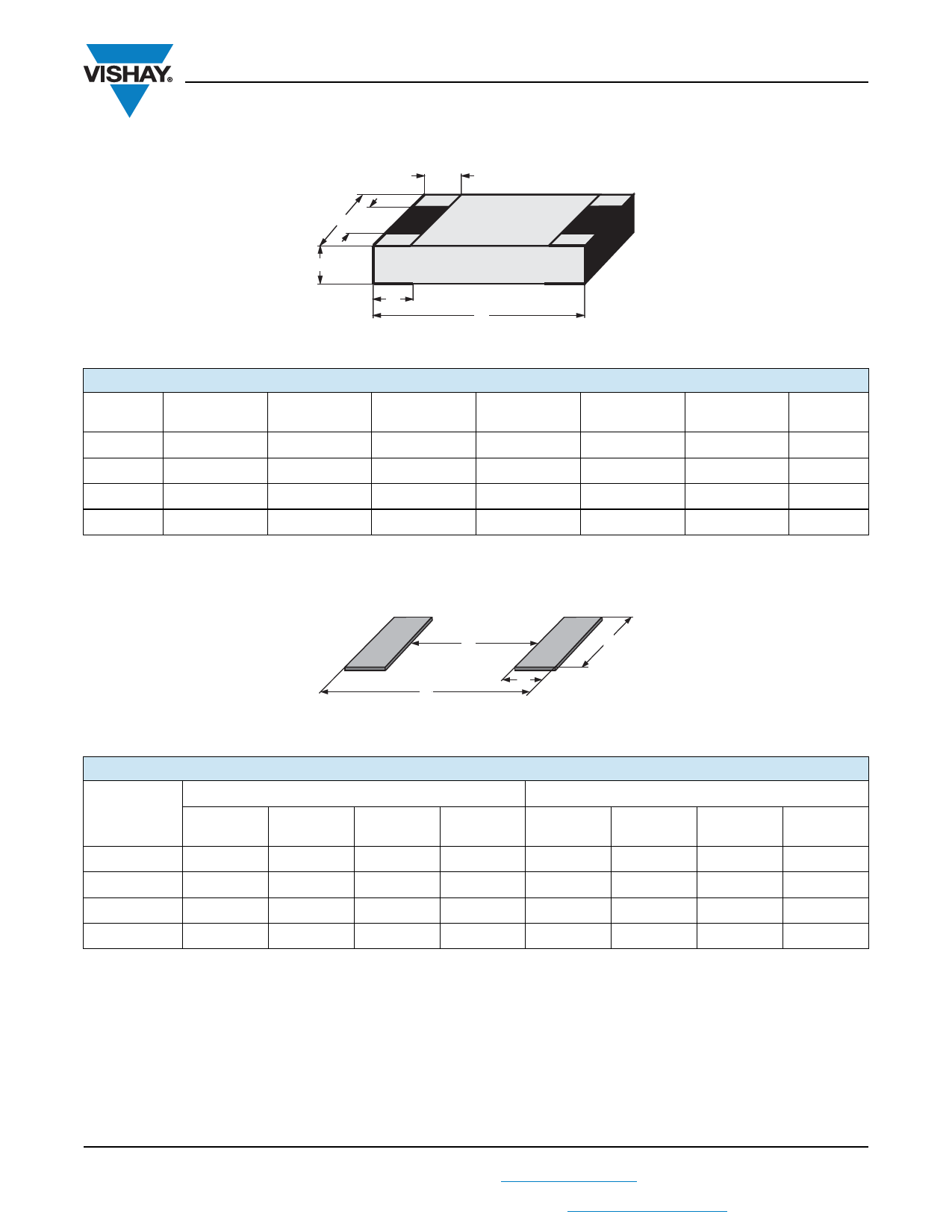
DIMENSIONS
Tt
W WT
H
Tb
L
DIMENSIONS AND MASS
TYPE
H
(mm)
L
(mm)
MCS 0402 0.32 ± 0.05
1.0 ± 0.05
MCT 0603 0.45 + 0.1/- 0.05 1.55 ± 0.05
MCU 0805 0.45 + 0.1/- 0.05
2.0 ± 0.1
MCA 1206
0.55 ± 0.1
3.2 + 0.1/- 0.2
W
(mm)
0.5 ± 0.05
0.85 ± 0.1
1.25 ± 0.15
1.6 ± 0.15
WT
(mm)
> 75 % of W
> 75 % of W
> 75 % of W
> 75 % of W
Tt
(mm)
Tb
(mm)
0.2 + 0.1/- 0.15
0.2 ± 0.1
0.3 + 0.15/- 0.2 0.3 + 0.15/- 0.2
0.4 + 0.1/- 0.2 0.4 + 0.1/- 0.2
0.5 ± 0.25
0.5 ± 0.25
MASS
(mg)
0.6
1.9
4.6
9.2
SOLDER PAD DIMENSIONS
G
X
Y
Z
RECOMMENDED SOLDER PAD DIMENSIONS
TYPE
G
(mm)
WAVE SOLDERING
Y
(mm)
X
(mm)
Z
(mm)
G
(mm)
REFLOW SOLDERING
Y
(mm)
X
(mm)
Z
(mm)
MCS 0402
-
-
-
-
0.35
0.55
0.55
1.45
MCT 0603
0.55
1.10
1.10
2.75
0.65
0.70
0.95
2.05
MCU 0805
0.80
1.25
1.50
3.30
0.90
0.90
1.40
2.70
MCA 1206
1.40
1.50
1.90
4.40
1.50
1.15
1.75
3.80
Note
• The rated dissipation applies only if the permitted film temperature is not exceeded. Furthermore, a high level of ambient temperature or of
power dissipation may raise the temperature of the solder joint, hence special solder alloys or board materials may be required to maintain
the reliability of the assembly.
Specified power rating above 125 °C requires dedicated heat-sink pads, which depend on board materials.
The given solder pad dimensions reflect the considerations for board design and assembly as outlined e.g. in standards IEC 61188-5-x, or
in publication IPC-7351. They do not guarantee any supposed thermal properties, particularly as these are also strongly influenced by many
other parameters.
Still, the given solder pad dimensions will be found adequate for most general applications, e.g. those referring to “standard operation
mode”. Please note however that applications for “power operation mode” require special considerations for the design of solder pads and
adjacent conductor areas.
Revision: 24-Jan-13
3
Document Number: 28705
For technical questions, contact: thinfilmchip@vishay.com
THIS DOCUMENT IS SUBJECT TO CHANGE WITHOUT NOTICE. THE PRODUCTS DESCRIBED HEREIN AND THIS DOCUMENT
ARE SUBJECT TO SPECIFIC DISCLAIMERS, SET FORTH AT www.vishay.com/doc?91000
Share Link: 