LTC1514 Просмотр технического описания (PDF) - Linear Technology
Номер в каталоге
Компоненты Описание
производитель
LTC1514
Linear Technology

LTC1514 Datasheet PDF : 8 Pages
| |||
LTC1514-3.3/LTC1514-5
APPLICATIONS INFORMATION
output pin cause high frequency voltage spikes on VOUT
with every clock cycle.
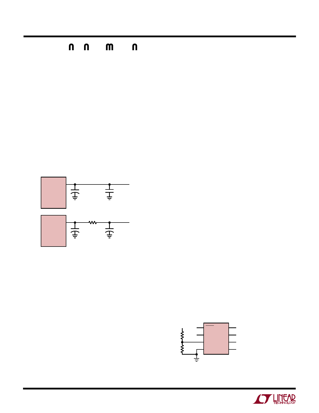
There are several ways to reduce the output voltage
ripple. A larger COUT capacitor (22µF or greater) will
reduce both the low and high frequency ripple due to the
lower COUT charging and discharging dV/dt and the lower
ESR typically found with higher value (larger case size)
capacitors. A low ESR ceramic output capacitor will
minimize the high frequency ripple, but will not reduce
the low frequency ripple unless a high capacitance value
is chosen. A reasonable compromise is to use a 10µF to
22µF tantalum capacitor in parallel with a 1µF to 3.3µF
ceramic capacitor on VOUT to reduce both the low and
high frequency ripple. An RC or LC filter may also be used
to reduce high frequency voltage spikes (see Figure 1).
8
VOUT +
LTC1514-X
15µF
TANTALUM
VOUT
1µF
CERAMIC
8
VOUT +
LTC1514-X
2Ω
10µF
TANTALUM
+
10µF
VOUT
TANTALUM
1514 F01
Figure 1. Output Ripple Reduction Techniques
Inrush Currents
A common problem with switched capacitor regulators
is inrush current — particularly during power-up and
coming out of shutdown mode. Whenever large VIN (or
boosted VIN) to VOUT voltage differentials are present,
most charge pumps will pull large current spikes from
the input supply. Only the effective charge pump output
impedance limits the current while the charge pump is
enabled. This may disrupt input supply regulation, espe-
cially if the input supply is a low power DC/DC converter
or linear regulator. The LTC1514-3.3/LTC1514-5 mini-
mize inrush currents both at start-up and under normal
high VIN to VOUT operation.
Internal soft start circuitry controls the rate at which VOUT
may be charged from 0V to its final regulated value. The
typical start-up time from VOUT = 0V to 5V is 4ms. This
corresponds to an effective VOUT charging current of only
12.5mA for a 10µF output capacitor (27.5mA for 22µF,
etc). Note that any output current load present during
start-up will add directly to the charging currents men-
tioned above. The soft start circuitry limits start-up
current both at initial power-up and when coming out of
shutdown.
As the VIN (or boosted VIN) to VOUT voltage differential
grows, the effective output impedance of the charge
pump is automatically increased by internal voltage
sensing circuitry. This feature minimizes the current
spikes pulled from VIN whenever the charge pump is
enabled and helps to reduce both input and output ripple.
Protection Features
The LTC1514-X contain thermal shutdown and short-
circuit protection features. The parts will shut down when
the junction temperature reaches approximately 150°C
and will resume operation once the junction temperature
has dropped back to approximately 140°C. The parts will
limit output current to 12mA (typ) when a short-circuit
condition (VOUT < 100mV) exists. The parts can survive
an indefinite short to GND. The LTC1514-X devices use
a low thermal resistance SO-8 package (110°C/W vs
150°C/W for standard SO-8). This permits full output
current, even at high input supply voltages.
Low-Battery Comparator
The internal low-battery comparator trips at 1.145 ±3%
(LBI ramping negative). Programming the comparator to
trip at a higher voltage can easily be done with an external
VBAT
R1
R2
LTC1514-X
1
SHDN
2
LBO
3
LBI
4
GND
8
VOUT
7
VIN
C1+ 6
C1– 5
1514 F02
VTRIP = 1.145V(1 + R1/R2)
(LBI RAMPING NEGATIVE)
Figure 2. Programming the Low-Battery Comparator Trip Voltage
6
Share Link: