TEA1024 Просмотр технического описания (PDF) - Temic Semiconductors
Номер в каталоге
Компоненты Описание
производитель
TEA1024 Datasheet PDF : 8 Pages
| |||
TEA1024/ TEA1124
Power Supply and its Limitations
Full-Wave Logic
The voltage limitation contained in the IC allows it to be
ă powered from mains via series resistance R1 and recti–
fying diode D1 between Pin 6 (+ Pol/ ) and Pin 4 (–VS).
The capacitor C1 smooths the supply voltage
(see figure 1).
An internal temperature-compensated limiting circuit
protects the module from random peaks of voltage on the
mains, and delivers a defined reference voltage during the
negative half-cycle.
Synchronization
The full-wave logic ensures that only pairs of pulses can
be released, and that these always begin with the positive
dv/dt. The load is thus switched on for a minimum of one
complete mains cycle. This means that the triac receives
a minimum of two driving pulses, so that the unwanted
d.c. component in the load circuit is definitely eliminated.
Pulse Amplifier
The pulse amplifier connected to the output of the full-
wave logic circuit, is proof against continuos
short-circuits, and delivers negative output pulses of typ.
75 mA, via an integrated limiting resistance, to Pin 5.
Ramp Generator (Figures 3, 4)
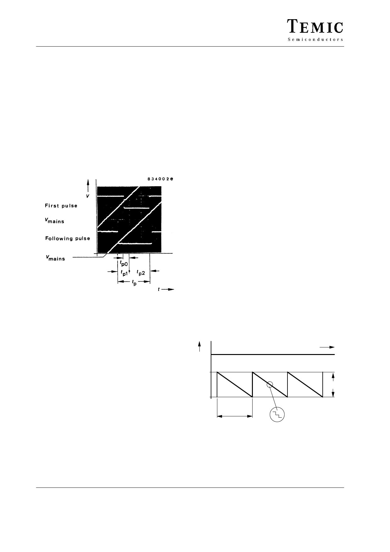
Figure 2. Pulse position optimization
The logic function is synchronized by means of a separate
resistance R2 connected between Pin 7 and phase
(voltage-synchronization). The width of the pulse can be
varied between wide limits by choice of Rsync. The larger
the value chosen, the wider the output pulse is on Pin 5.
Automatic optimization of the phase of the pulse is
necessary, since the latching current of the triac exceeds
the steady current by a factor of 3.
Ramp voltage which is generated in the IC is available not
only at reference Pin 1, but also at the non-inverted input
of the comparator.
The current sink which is controlled by D/A converter
influences the internal reference voltage at Pin 1 specified
by voltage divider. The current sink is turned-off in the
reset state of the D/A converter so that the voltage at Pin 1
is primarily specified via the internal voltage divider
(ramp starting voltage).
In the maximum state of the 4 stage (5 stage – TEA1124)
D/A converter, the current sink overtakes the maximum
current, whereby the ramp’s final (end) voltage has
reached. External resistance Rx, Ry shown in figure 4 are
in position to influence the initial ramp voltage as well as
the ramp amplitude. If the external resistances ratio Rx,
Ry is the same as that of the internal ratio, the ramp
voltage at the beginning remains maintained (constant),
only the amplitude is compressed.
V1
–1.3 V
t
2.2 V
The phase of the pulse is chosen so that ca. 1/3 of the pulse –3.8 V
width appears before the transition through null and 2/3
T= 640 ms
after it (see electrical characteristics and figure 2).
(T= 1280 ms)
16 stage ramp
In order to avoid phase-clipping after the switch-on the 95 11410
first third of the first pulse is automatically suppressed.
Figure 3. Ramp diagram without external circuit
2 (8)
TELEFUNKEN Semiconductors
Rev. A1, 24-May-96
Share Link: 