IL4116(1999) Просмотр технического описания (PDF) - Infineon Technologies
Номер в каталоге
Компоненты Описание
производитель
IL4116 Datasheet PDF : 3 Pages
| |||
FEATURES
• High Input Sensitivity: IFT=1.3 mA, PF=1.0; IFT=3.5 mA,
Typical PF < 1.0
• Zero Voltage Crossing
• 600/700/800 V Blocking Voltage
• 300 mA On-State Current
• High Static dv/dt 10,000 V/µsec., typical
• Inverse Parallel SCRs Provide Commutating
dv/dt>10 kV/msec.
• Very Low Leakage <10 µA
• Isolation Test Voltage from Double Molded Package
5300 VACRMS
• Package, 6-Pin DIP
• Underwriters Lab File #E52744
DESCRIPTION
The IL411x consists of an AlGaAs IRLED optically coupled to
a photosensitive zero crossing TRIAC network. The TRIAC
consists of two inverse parallel connected monolithic SCRs.
These three semiconductors are assembled in a six pin 0.3
inch dual in-line package, using high insulation double
molded, over/under leadframe construction.
High input sensitivity is achieved by using an emitter follower
phototransistor and a cascaded SCR predriver resulting in
an LED trigger current of less than 1.3 mA(DC).
The IL411x uses two discrete SCRs resulting in a commutat-
ing dV/dt greater than 10 kV/ms The use of a proprietary dv/
dt clamp results in a static dv/dt of greater than 10 kV/µs.
This clamp circuit has a MOSFET that is enhanced when
high dv/dt spikes occur between MT1 and MT2 of the
TRIAC. When conducting, the FET clamps the base of the
phototransistor, disabling the first stage SCR predriver.
The zero cross line voltage detection circuit consists of two
enhancement MOSFETS and a photodiode. The inhibit volt-
age of the network is determined by the enhancement volt-
age of the N-channel FET. The P-channel FET is enabled by
a photocurrent source that permits the FET to conduct the
main voltage to gate on the N-channel FET. Once the main
voltage can enable the N-channel, it clamps the base of the
phototransistor, disabling the first stage SCR predriver.
The blocking voltage of up to 800 V permits control of off-line
voltages up to 240 VAC, with a safety factor of more than
two, and is sufficient for as much as 380 VAC. Current han-
dling capability is up to 300 mA RMS continuous at 25°C.
The IL411x isolates low-voltage logic from 120, 240, and 380
VAC lines to control resistive, inductive, or capacitive loads
including motors, solenoids, high current thyristors or TRIAC
and relays.
Applications include solid-state relays, industrial controls,
office equipment, and consumer appliances.
600 V IL4116
700 V IL4117
800 V IL4118
Zero Voltage Crossing
Triac Driver Optocoupler
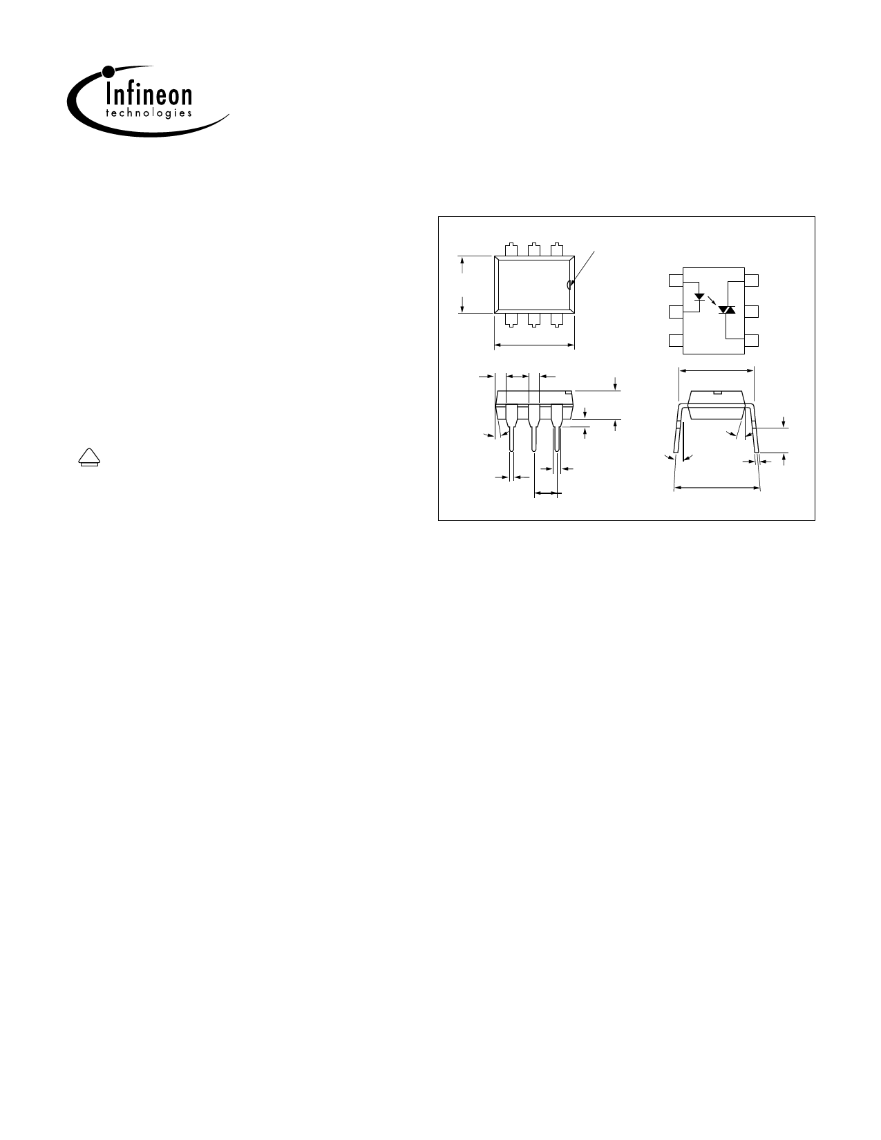
Dimensions in inches (mm)
321
pin one ID
.248 (6.30)
.256 (6.50)
.039
(1.00)
Min.
4°
typ.
.018 (0.45)
.022 (0.55)
4 56
.335 (8.50)
.343 (8.70)
.048 (0.45)
.022 (0.55)
LED 1
Anode
LED
Cathode 2
NC 3
6
Triac
MT2
Substrate
5 do not
connect
4
Triac
MT1
.300 (7.62)
typ.
.130 (3.30)
.150 (3.81)
.031 (0.80) min. 3°–9°
.031 (0.80)
.035 (0.90)
.100 (2.54) typ.
18°
.010 (.25)
typ.
.300–.347
(7.62–8.81)
.114 (2.90)
.130 (3.0)
Maximum Ratings
Emitter
Reverse Voltage .....................................................................6.0 V
Forward Current....................................................................60 mA
Surge Current .........................................................................2.5 A
Power Dissipation ..............................................................100 mW
Derate Linearly from 25°C ...........................................1.33 mW/°C
Thermal Resistance .........................................................750 °C/W
Detector
Peak Off-State Voltage
IL4116 ................................................................................600 V
IL4117 ................................................................................700 V
IL4118 ................................................................................800 V
RMS On-State Current ........................................................300 mA
Single Cycle Surge .................................................................3.0 A
Total Power Dissipation .....................................................500 mW
Derate Linearly from 25°C .............................................6.6 mW/°C
Thermal Resistance ..........................................................150°C/W
Package
Lead Soldering Temperature.................................. 260°C/5.0 sec.
Creepage Distance .......................................................... ≥7.0 mm
Clearance ......................................................................... ≥7.0 mm
Storage Temperature...........................................–55°C to +150°C
Operating Temperature .......................................–55°C to +100°C
Isolation Test Voltage ....................................................5300 VRMS
Isolation Resistance
VIO=500 V, TA=25°C ...................................................... ≥1012 Ω
VIO=500 V, TA=100°C .................................................... ≥1011 Ω
Infineon Technologies, Corp. • Optoelectronics Division • Cupertino, CA (formerly Siemens Microelectronics, Inc.)
www.infineon.com/opto • 1-800-777-4363
1
June 24, 1999
Share Link: 