WS27C256L Просмотр технического описания (PDF) - STMicroelectronics
Номер в каталоге
Компоненты Описание
производитель
WS27C256L Datasheet PDF : 5 Pages
| |||
WS27C256L
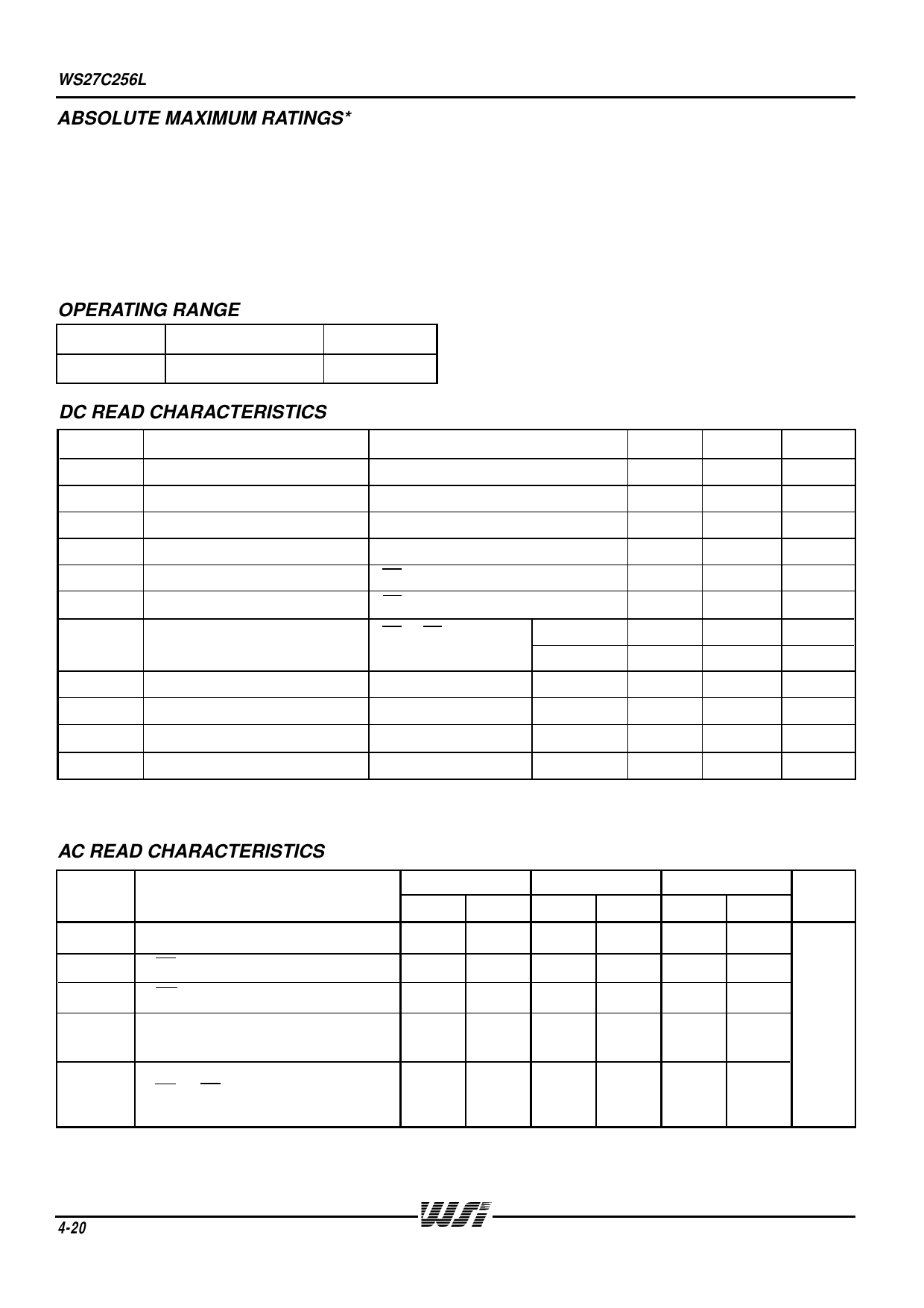
ABSOLUTE MAXIMUM RATINGS*
Storage Temperature............................–65° to + 150°C
Voltage on any Pin with
Respect to Ground ....................................–0.6V to +7V
VPP with Respect to Ground...................–0.6V to + 14V
VCC Supply Voltage with
Respect to Ground ....................................–0.6V to +7V
ESD Protection ..................................................>2000V
OPERATING RANGE
RANGE
TEMPERATURE
Military
–55°C to +125°C
VCC
+5V ± 10%
*NOTICE:
Stresses above those listed under "Absolute Maximum
Ratings" may cause permanent damage to the device.
This is a stress rating only and functional operation of
the device at these or any other conditions above
those indicated in the operational sections of this
specification is not implied. Exposure to absolute
maximum rating conditions for extended periods of
time may affect device reliability.
DC READ CHARACTERISTICS Over Operating Range. (See Above)
SYMBOL
PARAMETER
TEST CONDITIONS
MIN
MAX
VIL
Input Low Voltage
VIH
Input High Voltage
VOL
Output Low Voltage
VOH
Output High Voltage
IOL = 2.1 mA
IOH = –400 µA
–0.5
2.0
3.5
0.8
VCC + 1
0.4
ISB1
VCC Standby Current (CMOS) CE = VCC ± 0.3 V (Note 2)
100
ISB2
VCC Standby Current
CE = VIH
1
ICC
VCC Active Current
CE = OE = VIL
(Note 1)
F = 5 MHz
F = 8 MHz
40
50
IPP
VPP Supply Current
VPP
VPP Read Voltage
ILI
Input Leakage Current
VPP = VCC
VIN = 5.5 V or Gnd
100
VCC –0.4
VCC
–10
10
ILO
Output Leakage Current
VOUT = 5.5 V or Gnd
–10
10
NOTES: 1. The supply current is the sum of ICC and IPP. The maximum current value is with Outputs O0 to O7 unloaded.
2. CMOS inputs: VIL = GND ± 0.3V, VIH = VCC ± 0.3 V.
UNITS
V
V
V
V
µA
mA
mA
mA
µA
V
µA
µA
AC READ CHARACTERISTICS Over Operating Range (See Above)
SYMBOL
PARAMETER
WS27C256L-12 WS27C256L-15 WS27C256L-20
UNITS
MIN
MAX
MIN
MAX
MIN
MAX
t ACC
t CE
tOE
t DF
Address to Output Delay
CE to Output Delay
OE to Output Delay
Output Disable to Output Float
(Note 3)
120
150
200
120
150
200
35
40
40
ns
35
40
40
Output Hold From Addresses,
t OH
CE or OE, Whichever Occurred
0
0
0
First (Note 3)
NOTE: 3. This parameter is only sampled and is not 100% tested. Output Float is defined as the point where data is no longer driven – see timing
diagram.
4-20
Share Link: 