FX909AD2 Просмотр технического описания (PDF) - CML Microsystems Plc
Номер в каталоге
Компоненты Описание
производитель
FX909AD2 Datasheet PDF : 47 Pages
| |||
Wireless Modem Data Pump
FX909A
1.5 General Description
This product has been designed to be compliant with the appropriate sections of the "Mobitex
Interface Specification".
1.5.1 Description of Blocks
1.5.1.1
Data Bus Buffers
8 bidirectional 3-state logic level buffers between the modem's internal registers and the host µC's
data bus lines.
1.5.1.2
Address and R/W Decode
This block controls the transfer of data bytes between the µC and the modem's internal registers,
according to the state of the Write and Read Enable inputs (WRN and RDN), the Chip Select input
(CSN) and the Register Address inputs A0 and A1.
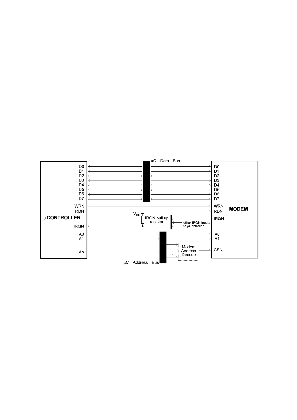
The Data Bus Buffers, Address and R/W Decode blocks provide a byte-wide parallel µC interface,
which can be memory-mapped, as shown in Figure 3.
Figure 3 Typical Modem µC Connections
1.5.1.3
Status and Data Quality Registers
8-bit registers which the µC can read to determine the status of the modem and the received data
quality.
1.5.1.4 Command, Mode and Control Registers
The values written by the µC to these 8-bit registers control the operation of the modem.
1.5.1.5 Data Buffer
An 18-byte buffer used to hold receive or transmit data to or from the µC.
© 1996 Consumer Microcircuits Limited
7
D/909A/4
Share Link: 