HFA3841 Просмотр технического описания (PDF) - Intersil
Номер в каталоге
Компоненты Описание
производитель
HFA3841 Datasheet PDF : 27 Pages
| |||
Preliminary - HFA3841
Absolute Maximum Ratings
Supply Voltage . . . . . . . . . . . . . . . . . . . . . . . . . . . . . . . . . . . . . . . .4V
Input, Output or I/O Voltage . . . . . . . . . . . . GND -0.5V to VCC +0.5V
ESD Classification . . . . . . . . . . . . . . . . . . . . . . . . . . . . . . . . . Class 2
Operating Conditions
Voltage Range . . . . . . . . . . . . . . . . . . . . . . . . . . . . +2.70V to +3.60V
Ambient Temperature Range . . . . . . . . . . . . . . . . . . . . . 0oC to 70oC
Thermal Information
Thermal Resistance (Typical, Note 1)
θJA (oC/W)
LQFP Package . . . . . . . . . . . . . . . . . . . . . . . . . . . . .
56
Maximum Storage Temperature Range . . . . . . . . . . -65oC to 150oC
Maximum Junction Temperature . . . . . . . . . . . . . . . . . . . . . . .100oC
Maximum Lead Temperature (Soldering 10s) . . . . . . . . . . . . .300oC
(Lead Tips Only)
CAUTION: Stresses above those listed in “Absolute Maximum Ratings” may cause permanent damage to the device. This is a stress only rating and operation of the
device at these or any other conditions above those indicated in the operational sections of this specification is not implied.
NOTE:
1. θJA is measured with the component mounted on an evaluation PC board in free air.
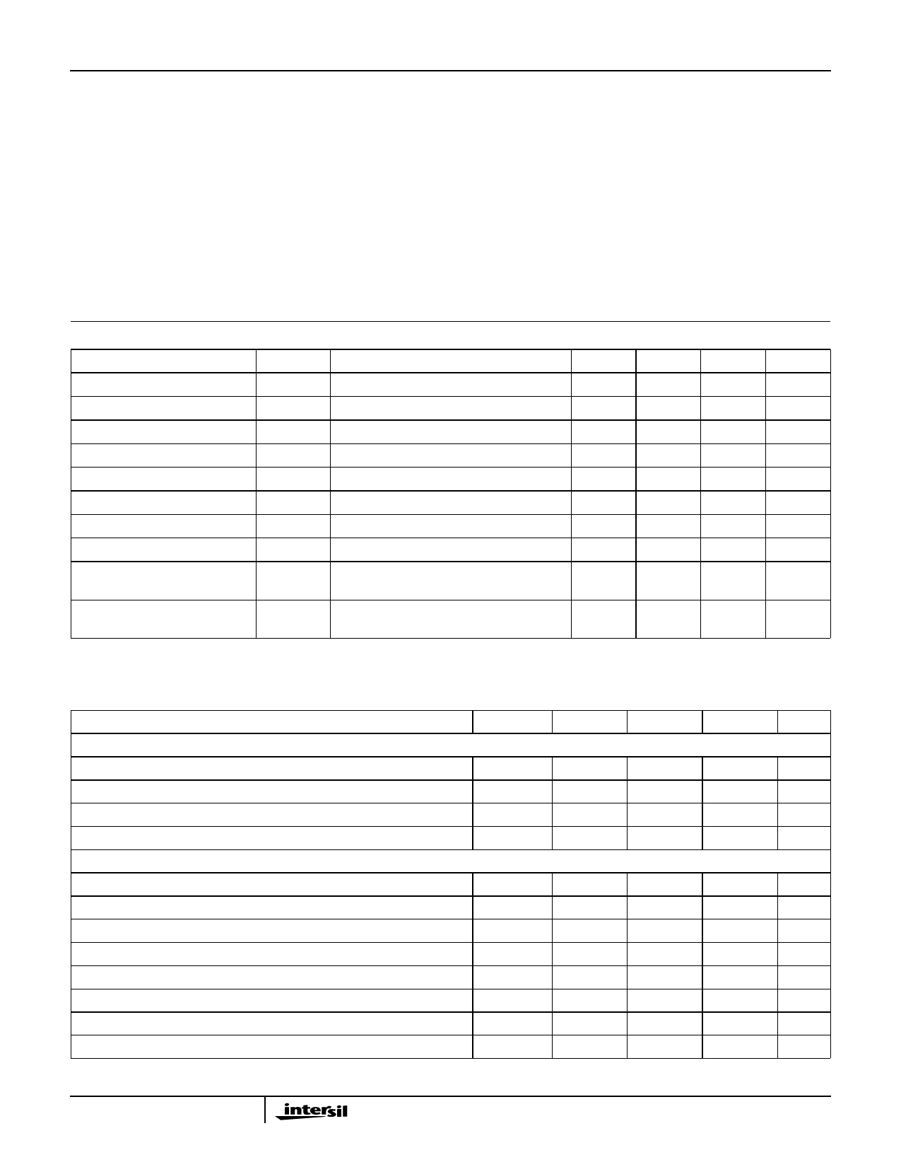
DC Electrical Specifications Maximum test temperature = 100oC, VCC = 3.0V to 3.3V ±10%, TA = -40oC to 85oC
PARAMETER
SYMBOL
TEST CONDITIONS
MIN
TYP
MAX
Power Supply Current
ICCOP VCC = 3.6V, CLK Frequency 44MHz
-
35
Standby Power Supply Current
ICCSB VCC = Max, Outputs not Loaded
-
0.5
Input Leakage Current
II
VCC = Max, Input = 0V or VCC
-10
1
Output Leakage Current
IO
VCC = Max, Input = 0V or VCC
-10
1
Logical One Input Voltage
VIH
VCC = Max, Min
0.7VCC
-
Logical Zero Input Voltage
VIL
VCC = Min, Max
-
-
Logical One Output Voltage
VOH
IOH = -1mA, VCC = Min
VCC-0.2
-
Logical Zero Output Voltage
VOL
IOL = 2mA, VCC = Min
-
0.2
Input Capacitance
CIN
CLK Frequency 1MHz. All measurements
referenced to GND. TA = 25oC
-
5
Output Capacitance
COUT
CLK Frequency 1MHz. All measurements
referenced to GND. TA = 25oC
-
5
NOTE: All values in this table have not been measured and are only estimates of the performance at this time.
45
1
10
10
-
VCC/3
-
0.2
10
10
UNITS
mA
mA
mA
mA
V
V
V
V
pF
pF
AC Electrical Specifications
PARAMETER
CLOCK SIGNAL TIMING
OSC Clock Period (Typ. 44MHz)
High Period
Low Period
Delay from OSC Edge to MCLK Edge
EXTERNAL MEMORY INTERFACE
Rising Edge MCLK to EMA[15:0], EMCSxN, EMOEN, EMWRN
Width EMOEN
EMD[15:0] Read Data Setup
EMD[15:0] Read Data Hold
Minimum Width between Read and Write
Width EMWRN
EMWRN Rising to EMCSxN Rising
EMD[15:0] Write Data Hold Time to Rising Edge EMWRN
SYMBOL
MIN
TYP
MAX
UNITS
tCYC
tH1
tL1
tD1
22
22.7
200
15
11.36
-
15
11.36
-
-
10
-
tD1
0
-
10
ns
tD2
2*tMCLK - 10
-
9*tMCLK + 10 ns
tS1
10
-
-
ns
tH1
-
-
0
ns
tD3
tMCLK - 10
tMCLK
tMCLK + 10
ns
tD4
2*tMCLK - 10
-
9*tMCLK + 10 ns
tD5
1*tMCLK - 10 1*tMCLK 1*tMCLK + 10 ns
tD6
1*tMCLK - 10 1*tMCLK 1*tMCLK + 10 ns
7
Share Link: 