HFA3841 Просмотр технического описания (PDF) - Intersil
Номер в каталоге
Компоненты Описание
производитель
HFA3841 Datasheet PDF : 27 Pages
| |||
Preliminary - HFA3841
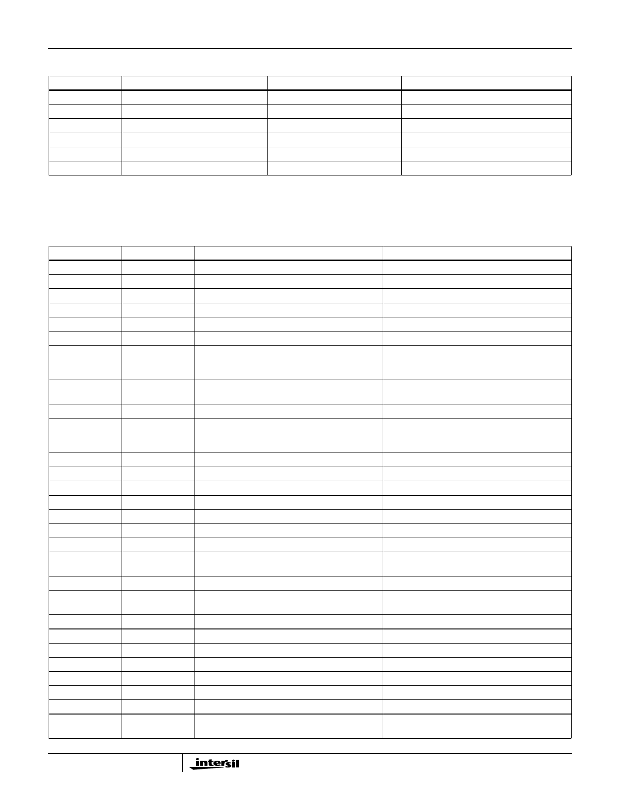
Power
PIN NAME
PIN NUMBER
PIN I/O TYPE
DESCRIPTION
VCC_CORE3
14, 25, 39, 53
3.3V Core Supply
VCC_IO3
66, 83, 98. 124
3.3V I/O Supply
VCC_IO5
105
5V Tolerance Supply
VSS_CORE3
VSS_IO3
TRST-
13, 24, 37
42, 52, 67, 82, 97, 115
62
Core VSS
I/O VSS
CMOS Input
Reserved - Must be tied low through 1K
ST = Schmitt Trigger (Hysteresis), TS = Three-State. Signals ending with “-” are active low.
NOTE: Output pins typically drive to positive voltage rail less 0.1V. Hence with a supply of 2.7V the output will just meet 5V TTL signal levels at
rated loads.
Port Pin Uses for PRISM Application
PIN
20
19
18
17
31
30
32
29
65
8
7
9
35
34
33
63
64
21
22
23
15
27
26
28
43
12
11
93
NAME
RXC
RXD
TXC
TXD
PJ0
PJ1
PJ2
PJ3
PJ4
PJ5
PJ6
PJ7
PK0
PK1
PK2
PK3
PK4
PK5
PK6
PK7
PL0
PL1
PL2
PL3
PL4
PL5
PL6
PL7
PRISM I USE
PRISM II™ USE
RXC - Receive clock
RXC - Receive clock
RXD - Receive data
RXD - Receive data
TXC - Transmit clock
TXC - Transmit clock
TXD - Transmit data
TXD - Transmit data
SCLK - Clock for the SD serial bus.
SCLK - Clock for the SD serial bus.
SD - Serial bi-directional data bus
SD - Serial bi-directional data bus
R/W - An input to the HFA3860A used to change Not Used
the direction of the SD bus when reading or writing
data on the SD bus.
CS - A Chip select for the device to activate the se- CS_BAR - Chip select for HFA3861 baseband
rial control port. (active low)
(active low)
Not Used
PE1 - Power Enable 1
SYNTH_LE - Latches a frame of 22 bits after it has LE_IF - Load enable for HFA3783 Quad IF
been shifted by the SCLK into the synthesizer reg-
isters.
LED - Activity indicator
LED - Activity indicator
Not Used
RADIO_PE - RF power enable
Not Used
LE_RF - Load enable for HFA3983 RF chip
Not Used
SYNTHCLK - Serial clock to front end chips
Not Used
SYNTHDATA - Serial data to front end chips
TX_PE_RF - Power Enable
PA_PE - Transmit PA power enable
RX_PE_RF - Power Enable
PE2 - Power Enable 2
MD_RDY - Header data and data packet are ready MDREADY - Header data and data packet are
to be transferred from Baseband on RXD
ready to be transferred from Baseband on RXD
CCA - Signal that the channel is clear to transmit. CCA - Signal that the channel is clear to transmit.
RADIO_PE - Master power control for the RF
section
CAL_EN - Calibration mode enable
TX_PE and PA_PE - Transmit Enable to Baseband TX_PE - Transmit Enable to Baseband
RX_PE - Receive Enable to Baseband
RX_PE - Receive Enable to Baseband
RESET - Reset to Baseband
RESET_BB - Reset Baseband
Not Used
T/R-SW_BAR - Transient/Receive Control (Inverted)
MA19 (if required)
MA19 (if required)
MA20 (if required)
MA20 (if required)
MA21 (if required)
Reserved
TX_RDY - Baseband ready to receive data on TXD T/R_SW - Transmit/Receive Control
(not used by firmware)
5
Share Link: 