M52348SP Просмотр технического описания (PDF) - MITSUBISHI ELECTRIC
Номер в каталоге
Компоненты Описание
производитель
M52348SP Datasheet PDF : 10 Pages
| |||
MITSUBISHI ICs (Monitor)
M52348SP
WIDE FREQUENCY BAND ANALOG SWITCH
8. When this is the case, calculate crosstalk C.T.I.2 between 2
inputs by the following formula:
C.T.I.2 = 20LOG
VOR4’
VOR4
[VP-P]
[VP-P]
(dB)
9. As in the same manner, find crosstalk between 2 pints in
response to input into pin 12 and pin 14 only.
C.T.I.3 Crosstalk 3 between 2 inputs
C.T.I.4 Crosstalk 4 between 2 inputs (100 MHz)
Specify input signal to be SG4. In the same manner as in C.T.I.1
and C.T.I.2, find crosstalk C.T.I.3/C.T.I.4 between 2 inputs.
C.T.C.1 Crosstalk 1 between channels
C.T.C.2 Crosstalk 2 between channels (10 MHz)
1. The conditions shall be as provided in the Electrical
Characteristics Table. This measurement shall take active
probe.
2. Assign SW17 to GND and input signal SG3 into pin 2 only.
Specify the output amplitude of T.P.31 to be VOR5 at that time.
3. In the same status, measure the output amplitude of T.P.28 and
T.P.25and specify the values to be VOG5 and VOB5.
4. When this is the case, calculate crosstalk C.T.C1 between
channels by the following formula:
C.T.C.1 = 20LOG
VOG5 or VOB5 [VP-P]
VOR5
[VP-P]
(dB)
5. In the same manner, find crosstalk between channels in
response to inputs into pin 4 and pin 6 only.
6. Assign SW17 to OPEN and then input signal SG3 into pin 10
only. Specify the output amplitude of T.P.31 to be VOR6 at that
time.
7. In the same status, measure the output amplitude of T.P.28 and
T.P.25. Specify the values to be VOG6 and VOB6.
8. When this is the case, calculate crosstalk C.T.C.2 between
channels by the following formula:
C.T.C.2 = 20LOG
VOG6 or VOB6 [VP-P]
VOR6
[VP-P]
(dB)
9. As in the same manner, find crosstalk between channels in
response to inputs into pin 12 and pin 14 only.
C.T.C.3 Crosstalk 3 between channels
C.T.C.4 Crosstalk 4 between channels (100 MHz)
Specify input signal to be SG4. In the same manner as in C.T.C.1
and C.T.C.2, find crosstalk C.T.C.3/C.T.C.4 between 2 channels.
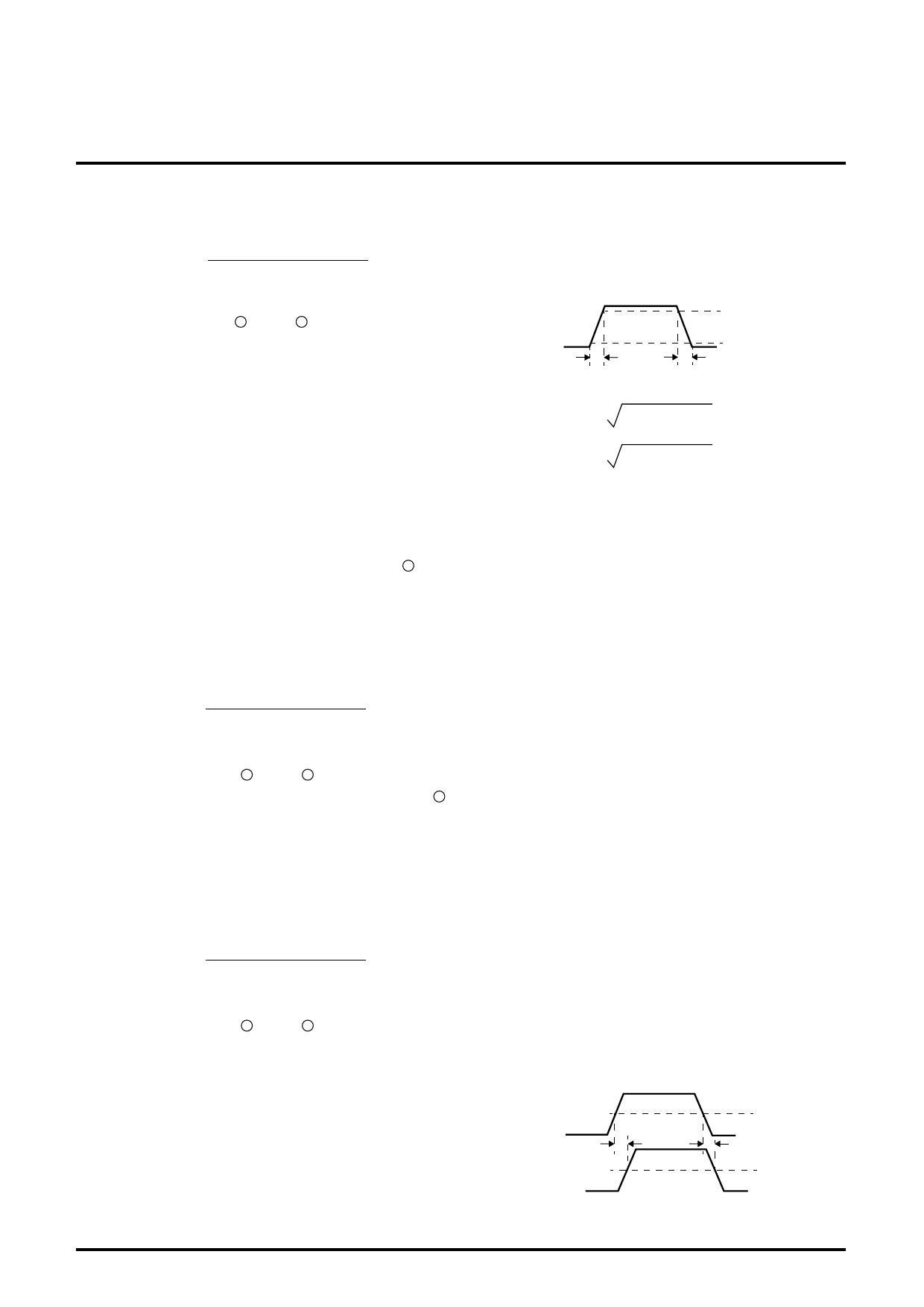
Tr1, Tf1, Tr2, Tf2 Pulse characteristics 1
and pulse characteristics 2
1. The conditions shall be as provided in the Electrical
Characteristics Table. Assign SW17 to GND (or OPEN).
2. With active probe, measure rising Tri and falling Tfi for 10% to
90% of the input pulse.
3. With active probe, measure rising Tro and falling Tfo for 10% to
90% of the output pulse.
4. The pulse characteristics Tr1 and Tf1 (Tr2 and Tf2) are as follows:
100%
90%
0%
Tr
10%
Tf
Tr1(Tr2) = (Tro)2 - (Tri)2 (nsec)
Tf1(Tf2) = (Tfo)2 - (Tfi)2 (nsec)
VOH1, VOH2 High-level output voltage 1 and high-level output
voltage 2
The conditions shall be as provided in the Electrical Characteristics
Table. Assign SW17 to GND (or OPEN), apply 5V to the input pin
and measure the output voltage. Specify the value to be VOH1
(VOH2).
VOL1, VOL2 Low-level output voltage 1 and low-level output
voltage 2
The conditions shall be as provided in the Electrical Characteristics
Table. Assign SW17 to GND (or OPEN), apply 0V to the input pin
and measure the output voltage. Specify the value to be VOL1
(VOL2).
Vith1 Input threshold voltage 1
Vith2 Input threshold voltage 2
The conditions shall be as provided in the Electrical Characteristics
Table. Assign SW17 to GND (or OPEN). Gradually increasing the
voltage of input pin from 0V, measure the input voltage when the
output voltage is Hi (4.5V or more). Specify the value to be Vith1
(Vith2).
Trd1, Trd2 Rising delay time 1 and rising delay time 2
Tfd1, Tfd2 Falling delay time 1 and falling delay time 2
The conditions shall be as provided in the Electrical Characteristics
Table. Assign SW17 to GND (or OPEN), input SG7 into the input
pin and measure the output waveform.
Rising delay time Trd1 (Trd2) and falling delay time Tfd1 (Tfd2) shall
be found according to the following diagram.
SG7
Trd
OOO
50%
Tfd
50%
5
Share Link: 