ML60852 Просмотр технического описания (PDF) - Oki Electric Industry
Номер в каталоге
Компоненты Описание
производитель
ML60852 Datasheet PDF : 81 Pages
| |||
1Semiconductor
PEDL60852-01
ML60852
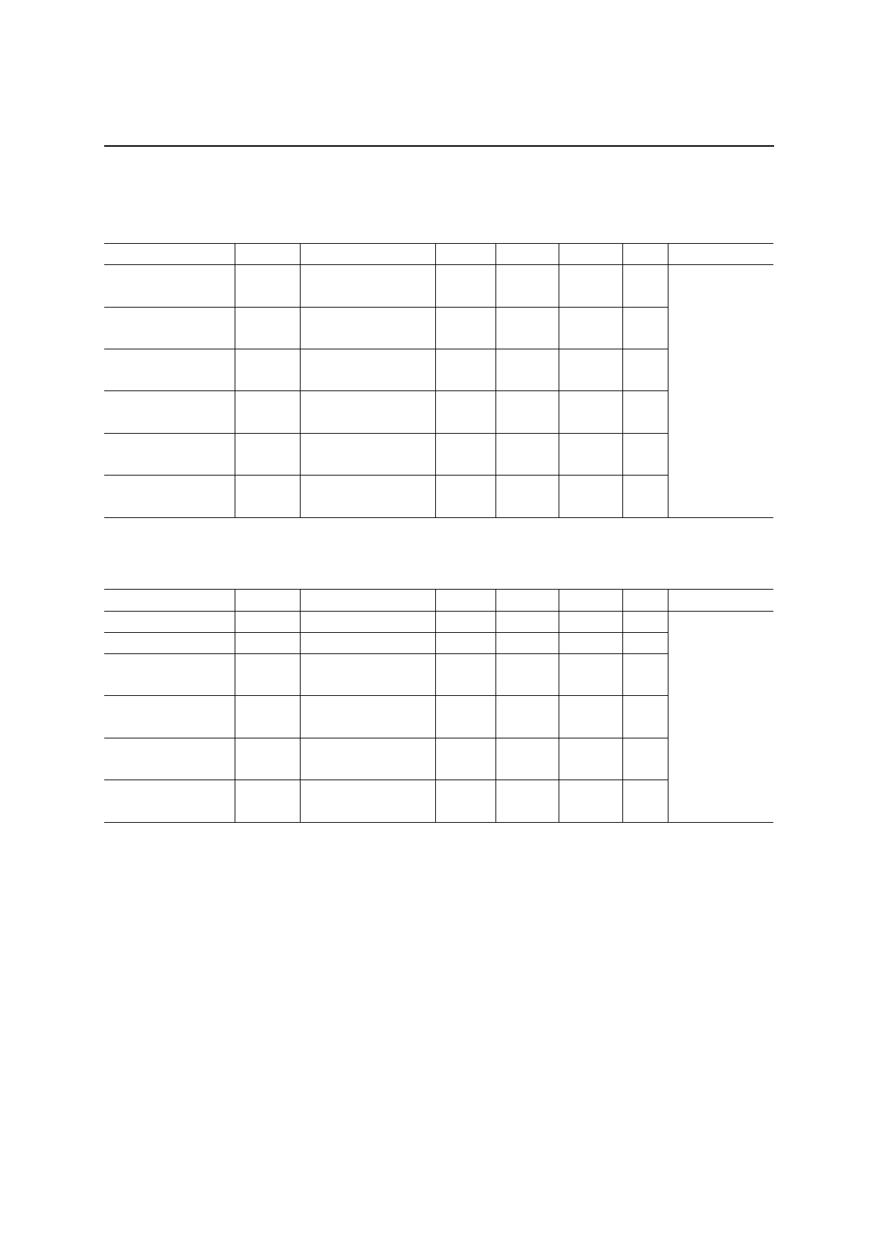
DC Characteristics (2) USB Port
Parameter
Symbol
Differential Input
Sensitivity
VDI
Differential Common
Mode Range
VCM
Single Ended
Receiver Threshold
VSE
High-level Output
Voltage
VOH
Low-level Output
Voltage
VOL
Output Leakage
Current
ILO
Condition
(D+) – (D –)
Includes VDI range
—
RL of 15 kΩ to GND
RL of 1.5 kΩ to 3.6 V
0 V <VIN <3.3 V
Min.
0.2
0.8
0.8
2.8
v
–10
(VCC = 3.0 to 3.6 V, Ta = 0 to +70 °C)
Typ.
Max. Unit Applicable pin
—
—
V
—
2.5
V
—
2.0
V
—
3.6
V
D+, D-
—
0.3
V
—
+10
µA
AC Characteristics USB Port
Parameter
Rise Time
Fall Time
Rise/Fall Time
Matching
Output Signal
Crossover Voltage
Driver Output
Resistance
Data Rate
Symbol
tR
tF
TRFM
Condition
CL = 50 pF
CL = 50 pF
(tR/ tF)
VCRS
—
ZDRV
TDRATE
Steady State Driver
Ave. Bit Rate
(12 Mbps ±0.25%)
Min.
4
4
90
1.3
28
11.97
Typ.
—
—
(VCC = 3.0 to 3.6 V, Ta = 0 to +70 °C)
Max. Unit Applicable pin
20
ns
20
ns
—
111.11 %
—
2
V
D+, D-
—
44
Ω
—
12.03
Mbp
s
Notes: 1. 1.5 kΩ pull-up to 3.3 V on the D + data line.
2. tR and tF are measured from 10% to 90% of the data signal.
9/81
Share Link: 