ADM8690AN Просмотр технического описания (PDF) - Analog Devices
Номер в каталоге
Компоненты Описание
производитель
ADM8690AN Datasheet PDF : 24 Pages
| |||
Data Sheet
ADM8690/ADM8691/ADM8695
CIRCUIT INFORMATION
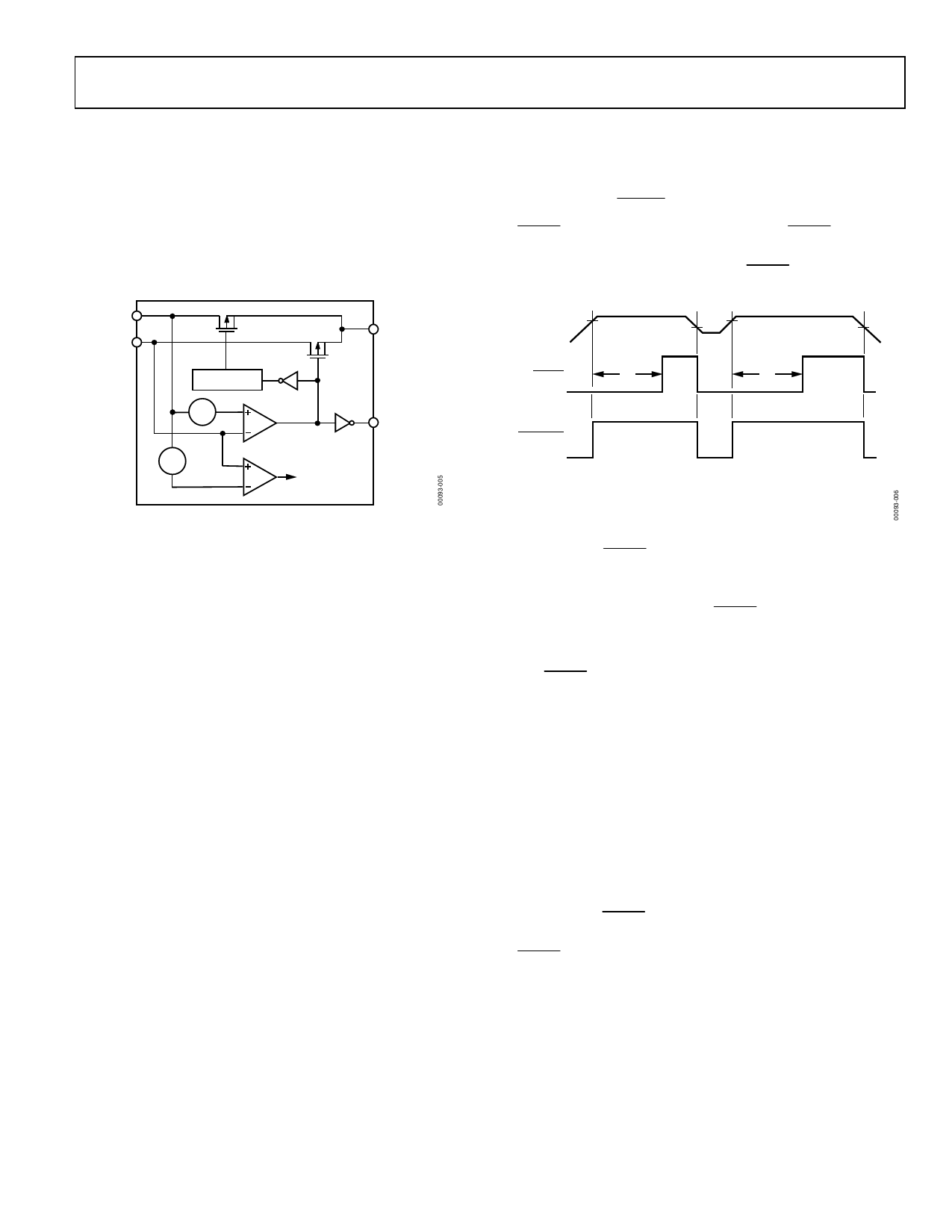
BATTERY SWITCHOVER SECTION
The battery switchover circuit compares VCC to the VBATT
input and connects VOUT to whichever is higher. Switchover
occurs when VCC is 50 mV higher than VBATT as VCC falls, and
when VCC is 70 mV greater than VBATT as VCC rises. This 20 mV
hysteresis prevents repeated rapid switching if VCC falls very
slowly or remains nearly equal to the battery voltage.
VCC
VBATT
VOUT
GATE DRIVE
100
mV
700
mV
INTERNAL
SHUTDOWN SIGNAL
WHEN
VBATT > (VCC + 0.7V)
BATT ON
(ADM8691,
ADM8695)
Figure 14. Battery Switchover Schematic
During normal operation, with VCC higher than VBATT, VCC
is internally switched to VOUT through an internal PMOS tran-
sistor switch. This switch has a typical on resistance of 0.7 Ω
and can supply up to 100 mA at the VOUT terminal. VOUT is
normally used to drive a RAM memory bank, requiring
instantaneous currents of greater than 100 mA. If this is the
case, a bypass capacitor should be connected to VOUT. The
capacitor provides the peak current transients to the RAM.
A capacitance value of 0.1 μF or greater can be used.
If the continuous output current requirements at VOUT exceed
100 mA or if a lower VCC − VOUT voltage differential is desired,
an external PNP pass transistor can be connected in parallel
with the internal transistor. The BATT ON output (ADM8691/
ADM8695) can directly drive the base of the external transistor
(see Figure 24).
A 7 Ω MOSFET switch connects the VBATT input to VOUT during
battery backup. This MOSFET has very low input-to-output
differential (dropout voltage) at the low current levels required
for battery backup of CMOS RAM or other low power CMOS
circuitry. The supply current in battery backup is typically 0.4 μA.
The ADM8690/ADM8691/ADM8695 operate with battery
voltages from 2.0 V to 4.25 V. High value capacitors, either standard
electrolytic or the farad-size, double-layer capacitors, can also be
used for short-term memory backup. A small charging current
of typically 10 nA (0.1 μA maximum) flows out of the VBATT
terminal. This current is useful for maintaining rechargeable
batteries in a fully charged condition. This extends the life of the
backup battery by compensating for its self-discharge current.
Also note that this current poses no problem when lithium
batteries are used for backup because the maximum charging
current (0.1 μA) is safe for even the smallest lithium cells.
If the battery switchover section is not used, VBATT should be
connected to GND and VOUT should be connected to VCC.
POWER-FAIL RESET OUTPUT
RESET is an active low output that provides a RESET signal to
the microprocessor whenever VCC is at an invalid level. When
VCC falls below the reset threshold, the RESET output is forced
low. The nominal reset voltage threshold is 4.65 V.
VCC
V2
V1
V2
V1
RESET
t1
t1
LOW LINE
t1 = RESET TIME
V1 = RESET VOLTAGE THRESHOLD LOW
V2 = RESET VOLTAGE THRESHOLD HIGH
HYSTERESIS = V2 – V1
Figure 15. Power-Fail Reset Timing
On power-up, RESET remains low for 50 ms (200 ms for the
ADM8695) after VCC rises above the appropriate reset thresh-
old. This allows time for the power supply and microprocessor
to stabilize. On power-down, the RESET output remains low
with VCC as low as 1 V. This ensures that the microprocessor is
held in a stable shutdown condition.
The RESET active time is adjustable on the ADM8691/
ADM8695 by using an external oscillator or by connecting an
external capacitor to the OSC IN pin. See Table 5 and Figure 17
through Figure 20.
The guaranteed minimum and maximum reset thresholds for
the ADM8690/ADM8691/ADM8695 are 4.5 V and 4.73 V. The
ADM8690/ADM8691/ADM8695 are, therefore, compatible with
5 V supplies with a +10%, −5% tolerance. The reset threshold
comparator typically has 40 mV of hysteresis. The response time
of the reset voltage comparator is less than 1 μs. If glitches are
present on the VCC line that could cause spurious reset pulses,
VCC should be decoupled close to the device.
In addition to RESET, the ADM8691/ADM8695 provide an
active high RESET output. This output is the complement of
RESET and is intended for processors that require an active
high reset signal.
Rev. C | Page 11 of 24
Share Link: 