80C42 Просмотр технического описания (PDF) - Intel
Номер в каталоге
Компоненты Описание
производитель
80C42 Datasheet PDF : 25 Pages
| |||
UPI-C42 UPI-L42
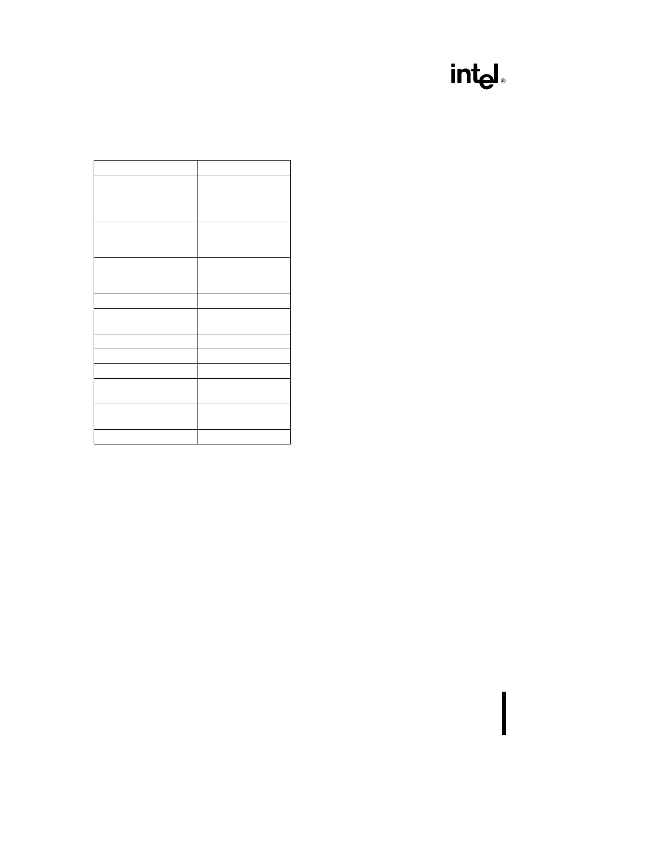
Table 2 covers all suspend mode pin states In addi-
tion to the suspend power down mode the UPI-C42
will also support the NMOS power down mode as
outlined in Chapter 4 of the UPI-42AH users manual
Table 2 Suspend Mode Pin States
Pins
Suspend
Ports 1 and 2
Outputs
Inputs
Tristate
Weak Pull-Up
Disabled
DBB(1)
Outputs
Inputs
Normal
Normal
System Control
(RD WR
CS A0)
Disabled
Reset
Enabled
Crystal Osc
(XTAL1 XTAL2)
Disabled
Test 0 Test 1
Disabled
Prog
High
Sync
High
EA
Disabled
No Pull-Up
SS
Disabled
Weak Pull-Up
ICC
k40 mA
NOTES
1 DBB outputs are Tristate unless CS and RD are ac-
tive DBB inputs are disabled unless CS and WR are
active
2 A ‘‘disabled’’ input will not cause current to be drawn
regardless of input level (within the supply range)
3 Weak pull-ups have current capability of typically 5 mA
NEW UPI-C42 INSTRUCTIONS
The UPI-C42 will support several new instructions to
allow for the use of new C42 features These in-
structions are not necessary to the user who does
not wish to take advantage of any new C42 function-
ality The C42 will be completely compatible with all
current NMOS code applications In order to use
new features however some code modifications will
be necessary All new instructions can easily be in-
serted into existing code by use of the ASM-48 mac-
ro facility as shown in the following example
Macname MACRO
DB 63H
ENDM
New Instructions
The following is a list of additions to the UPI-42 in-
struction set These instructions apply only to the
UPI-C42 These instructions must be added to exist-
ing code in order to use any new functionality
SEL PMB0 Select Program Memory Bank 0
OPCODE 0110 0011 (63h)
PC Bit 11 is set to zero on next JMP or CALL instruc-
tion All references to program memory fall within
the range of 0 – 2047 (0 – 7FFh)
SEL PMB1 Select Program Memory Bank 1
OPCODE 0111 0011 (73h)
PC Bit 11 is set to one on next JMP or CALL instruc-
tion All references to program memory fall within
the range of 2048 – 4095 (800h – FFFh)
ENA20 Enables Auto A20 hardware
OPCODE 0011 0011 (33h)
Enables on chip logic to support Hardware A20 Gate
feature Will remain enabled until device is reset
8
Share Link: 