80C42 Просмотр технического описания (PDF) - Intel
Номер в каталоге
Компоненты Описание
производитель
80C42 Datasheet PDF : 25 Pages
| |||
UPI-C42 UPI-L42
Table 1 Pin Description (Continued)
DIP PLCC
Symbol Pin
Pin
No
No
QFP
Pin
No
Type
Name and Function
P20 – P27 21 – 24 24 – 27 39 – 42
I O PORT 2 8-bit PORT 2 quasi-bidirectional I O lines The lower 4 bits
35– 38 39– 42 11 13– 15
(P20 – P23) interface directly to the 8243 I O expander device and
contain address and data information during PORT 4 – 7 access P21
can be programmed to provide hardware A20 gate support The upper
4 bits (P24 – P27) can be programmed to provide interrupt Request and
DMA Handshake capability Software control can configure P24 as
Output Buffer Full (OBF) interrupt P25 as Input Buffer Full (IBF)
interrupt P26 as DMA Request (DRQ) and P27 as DMA ACKnowledge
(DACK)
PROG
25
28
43
I O PROGRAM Multifunction pin used as the program pulse input during
PROM programming
During I O expander access the PROG pin acts as an address data
strobe to the 8243 This pin should be tied high if unused
VCC
40
44
17
VDD
26
29
1
POWER a5V main power supply pin
POWER a5V during normal operation a12 75V during programming
operation Low power standby supply pin
VSS
20
22
38
GROUND Circuit ground potential
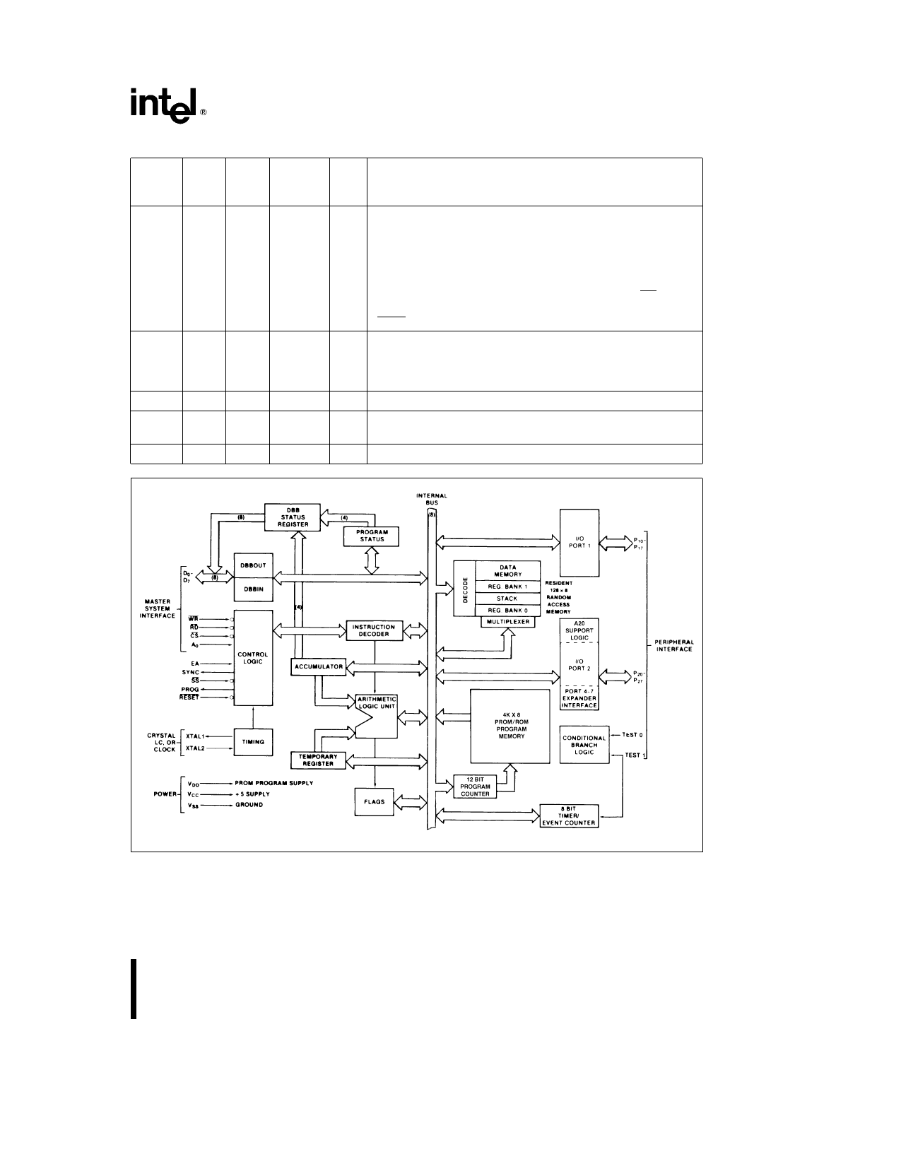
Figure 4 Block Diagram
290414 – 4
3
Share Link: 