MAX951 Просмотр технического описания (PDF) - Maxim Integrated
Номер в каталоге
Компоненты Описание
производитель
MAX951 Datasheet PDF : 13 Pages
| |||
MAX951–MAX954
Ultra-Low-Power, Single-Supply
Op Amp + Comparator + Reference
Absolute Maximum Ratings
Supply Voltage (VDD to VSS)...................................................9V
Inputs
Current (AMPIN_, COMPIN_).........................................20mA
Voltage (AMPIN_, COMPIN_)...(VDD + 0.3V) to (VSS - 0.3V)
Outputs
Current (AMPOUT, COMPOUT)......................................50mA
Current (REF)..................................................................20mA
Voltage (AMPOUT, COMPOUT,
REF)..........................................(VDD + 0.3V) to (VSS - 0.3V)
Short-Circuit Duration (REF, AMPOUT)..................Continuous
Short-Circuit Duration (COMPOUT, VDD to VSS ≤ 7V)...1min
Continuous Power Dissipation (TA = +70°C)
8-Pin Plastic DIP (derate 9.09mW/°C above +70°C)...727mW
8-Pin SO (derate 5.88mW/°C above +70°C)................471mW
8-Pin μMAX (derate 4.10mW/°C above +70°C)...........330mW
8-Pin CERDIP (derate 8.00mW/°C above +70°C).......640mW
Operating Temperature Ranges
MAX95_E_A ....................................................-40°C to +85°C
MAX95_MJA..................................................-55°C to +125°C
Maximum Junction Temperatures
MAX95_E_A.................................................................+150°C
MAX95_MJA.................................................................+175°C
Storage Temperature Range .............................-65°C to +165°C
Lead Temperature (soldering, 10s) .................................+300°C
Stresses beyond those listed under “Absolute Maximum Ratings” may cause permanent damage to the device. These are stress ratings only, and functional operation of the device at these
or any other conditions beyond those indicated in the operational sections of the specifications is not implied. Exposure to absolute maximum rating conditions for extended periods may affect
device reliability.
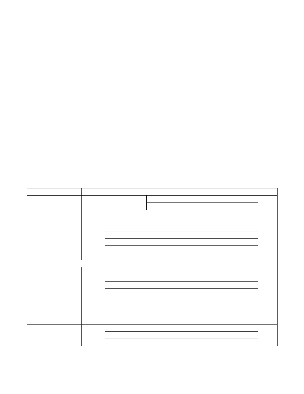
Electrical Characteristics
(VDD = 2.8V to 7V for MAX951/MAX952, VDD = 2.4V to 7V for MAX953/MAX954, VSS = 0, VCM COMP = 0 for the MAX953/MAX954,
VCM OPAMP = 0, AMPOUT = (VDD + VSS)/2, COMPOUT = low, TA = TMIN to TMAX, typical values are at TA = +25°C, unless other-
wise noted.)
PARAMETER
Supply Voltage Range
SYMBOL
CONDITIONS
VDD
MAX951/MAX952
MAX953/MAX954
TA = TMIN to TMAX
TA = -10°C to +85°C
MIN TYP MAX UNITS
2.8
7.0
2.7
7.0
V
2.4
7.0
TA = +25°C, MAX951/MAX952
MAX951E/MAX952E
7
10
11
Supply Current
(Note 1)
MAX951M/MAX952M
IS
TA = +25°C, MAX953/MAX954
MAX953E/MAX954E
13
µA
5
8
9
MAX953M/MAX954M
11
COMPARATOR
Input Offset Voltage
(Note 2)
TA = +25°C
MAX95_EPA/ESA
VOS
MAX95_EUA (μMAX)
1
3
14
mV
14
MAX95_MJA
6
Trip Point
(Note 3)
TA = +25°C
MAX95_EUA (μMAX)
MAX95_EPA/ESA
4
17
mV
5
MAX95_MJA
7
Input Leakage Current
(Note 4)
TA = +25°C
MAX95_E
MAX95_M
0.003 0.050
0.003
5
nA
40
www.maximintegrated.com
Maxim Integrated │ 2
Share Link: 