HI5905IN Просмотр технического описания (PDF) - Intersil
Номер в каталоге
Компоненты Описание
производитель
HI5905IN Datasheet PDF : 11 Pages
| |||
Pin Descriptions
PIN #
1
2
3
4
NAME
NC
NC
DGND1
NC
DESCRIPTION
No Connection
No Connection
Digital Ground
No Connection
5
AVCC Analog Supply (5.0V)
6
AGND Analog Ground
7
NC
No Connection
8
NC
No Connection
9
VIN+ Positive Analog Input
10
VIN- Negative Analog Input
11
VDC DC Bias Voltage Output
12
NC
No Connection
13
VROUT Reference Voltage Output
14
VRIN Reference Voltage Input
15
AGND Analog Ground
16
AVCC Analog Supply (5.0V)
17
NC
No Connection
18
D13 Data Bit 11 Output (MSB)
19
D12 Data Bit 11 Output
20
D11 Data Bit 11 Output
21
D10 Data Bit 10 Output
22
NC
No Connection
23
NC
No Connection
24
D9
Data Bit 9 Output
25
D8
Data Bit 8 Output
26
DGND2 Digital Ground
27
DVCC2 Digital Supply (5.0V)
28
NC
No Connection
29
D7
Data Bit 7 Output
30
D6
Data Bit 6 Output
31
D5
Data Bit 5 Output
32
D4
Data Bit 4 Output
33
D3
Data Bit 3 Output
34
NC
No Connection
35
NC
No Connection
36
D2
Data Bit 2 Output
37
D1
Data Bit 1 Output
38
D0
Data Bit 0 Output (LSB)
39
NC
No Connection
40
CLK Input Clock
41
DVCC1 Digital Supply (5.0V)
42
DGND1 Digital Ground
43
DVCC1 Digital Supply (5.0V)
44
NC
No Connection
7
HI5905
Detailed Description
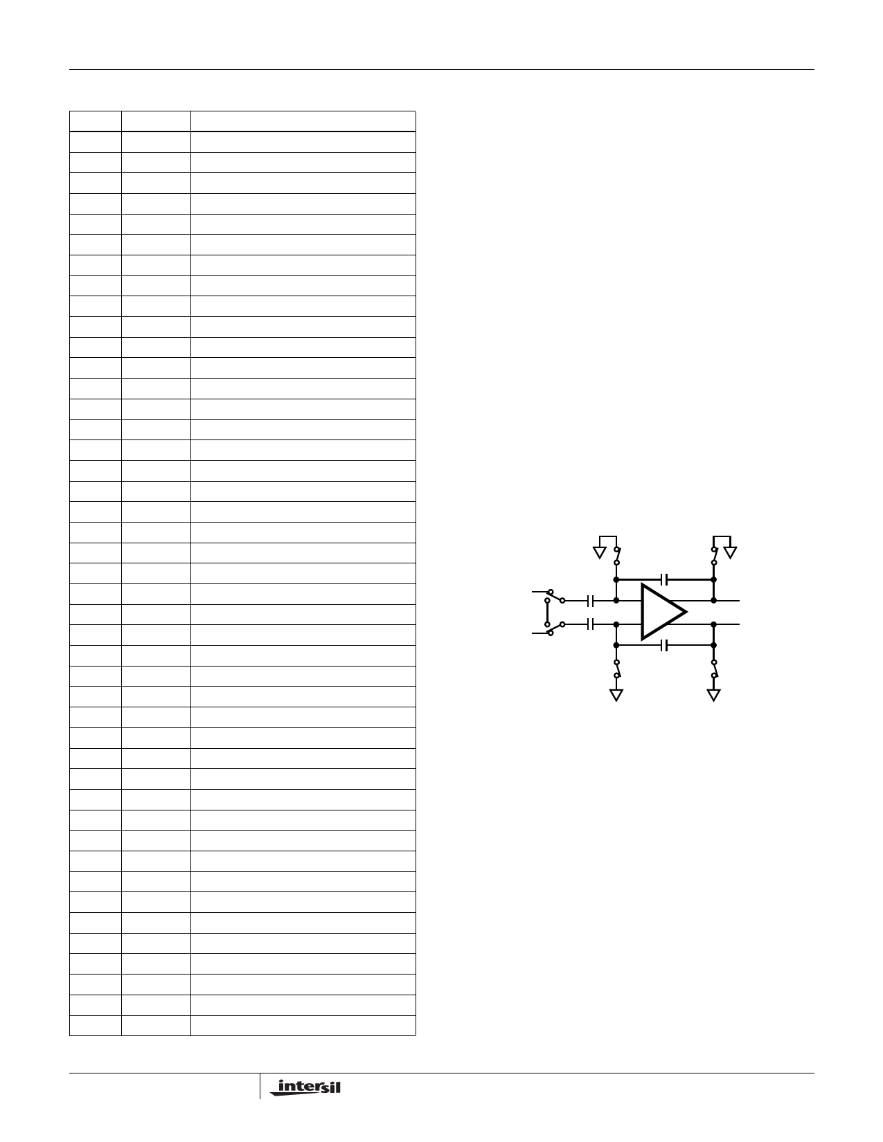
Theory of Operation
The HI5905 is a 14-bit fully differential sampling pipeline A/D
converter with digital error correction. Figure 8 depicts the
circuit for the front end differential-in-differential-out sample-
and-hold (S/H). The switches are controlled by an internal
clock which is a non-overlapping two phase signal, φ1 and
φ2 , derived from the master clock. During the sampling
phase, φ1 , the input signal is applied to the sampling
capacitors, CS . At the same time the holding capacitors, CH ,
are discharged to analog ground. At the falling edge of φ1
the input signal is sampled on the bottom plates of the
sampling capacitors. In the next clock phase, φ2 , the two
bottom plates of the sampling capacitors are connected
together and the holding capacitors are switched to the op-
amp output nodes. The charge then redistributes between
CS and CH completing one sample-and-hold cycle. The
output is a fully-differential, sampled-data representation of
the analog input. The circuit not only performs the sample-
and-hold function but will also convert a single-ended input
to a fully-differential output for the converter core. During the
sampling phase, the VIN pins see only the on-resistance of a
switch and CS . The relatively small values of these
components result in a typical full power input bandwidth of
100MHz for the converter.
φ 1 CH
VIN +
φ1
CS
-+
φ2
+-
VIN -
φ1
CS
φ1
CH
φ1
VOUT +
VOUT -
φ1
FIGURE 8. ANALOG INPUT SAMPLE-AND-HOLD
As illustrated in the functional block diagram and the timing
diagram in Figure 1, four identical pipeline subconverter stages,
each containing a four-bit flash converter, a four-bit digital-to-
analog converter and an amplifier with a voltage gain of 8,
follow the S/H circuit with the fifth stage being only a 4-bit flash
converter. Each converter stage in the pipeline will be sampling
in one phase and amplifying in the other clock phase. Each
individual sub-converter clock signal is offset by 180 degrees
from the previous stage clock signal, with the result that
alternate stages in the pipeline will perform the same operation.
The output of each of the four-bit subconverter stages is a
four-bit digital word containing a supplementary bit to be used
by the digital error correction logic. The output of each
subconverter stage is input to a digital delay line which is
controlled by the internal sampling clock. The function of the
digital delay line is to time align the digital outputs of the four
identical four-bit subconverter stages with the corresponding
output of the fifth stage flash converter before applying the
Share Link: 