HI5905EVAL2(1999) Просмотр технического описания (PDF) - Intersil
Номер в каталоге
Компоненты Описание
производитель
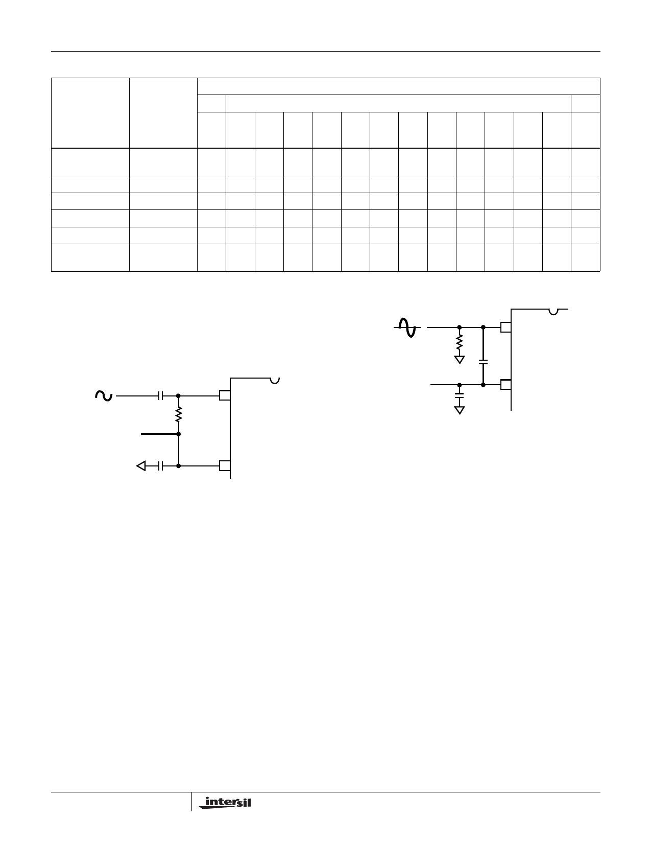
HI5905EVAL2 Datasheet PDF : 11 Pages
| |||
HI5905
VIN
VDC
VDC
-VIN
VIN+
R
C
HI5905
VDC
R
VIN-
FIGURE 10. DC COUPLED DIFFERENTIAL INPUT
The resistors, R, in Figure 10 are not absolutely necessary
but may be used as load setting resistors. A capacitor, C,
connected from VIN+ to VIN- will help filter any high fre-
quency noise on the inputs, also improving performance.
Values around 20pF are sufficient and can be used on AC
coupled inputs as well. Note, however, that the value of
capacitor C chosen must take into account the highest
frequency component of the analog input signal.
Analog Input, Single-Ended Connection
The configuration shown in Figure 11 may be used with a
single ended AC coupled input. Sufficient headroom must be
provided such that the input voltage never goes above +5V
or below AGND.
VIN
VIN+
VDC
HI5905
VIN-
FIGURE 11. AC COUPLED SINGLE ENDED INPUT
Again, the difference between the two internal voltage
references is 2V. If VIN is a 4VP-P sinewave, then VIN+ is a
4VP-P sinewave riding on a positive voltage equal to VDC. The
converter will be at positive full scale when VIN+ is at VDC + 2V
(VIN+ - VIN- = 2V) and will be at negative full scale when VIN+
is equal to VDC - 2V (VIN+ - VIN- = -2V). In this case, VDC
could range between 2V and 3V without a significant change in
ADC performance. The simplest way to produce VDC is to use
the VDC bias voltage output of the HI5905.
The single ended analog input can be DC coupled (Figure
12) as long as the input is within the analog input common
mode voltage range.
VIN
VDC
VIN+
R
C
HI5905
VDC
VIN -
FIGURE 12. DC COUPLED SINGLE ENDED INPUT
The resistor, R, in Figure 12 is not absolutely necessary but
may be used as a load setting resistor. A capacitor, C, con-
nected from VIN+ to VIN- will help filter any high frequency
noise on the inputs, also improving performance. Values
around 20pF are sufficient and can be used on AC coupled
inputs as well. Note, however, that the value of capacitor C
chosen must take into account the highest frequency com-
ponent of the analog input signal.
A single ended source will give better overall system
performance if it is first converted to differential before
driving the HI5905.
Digital I/O and Clock Requirements
The HI5905 provides a standard high-speed interface to
external TTL/CMOS logic families. The digital CMOS clock
input has TTL level thresholds. The low input bias current
allows the HI5905 to be driven by CMOS logic. The digital
CMOS outputs have a separate +5.0V digital supply input pin.
In order to ensure rated performance of the HI5905, the duty
cycle of the clock should be held at 50% ±5%. It must also
have low jitter and operate at standard TTL levels.
Performance of the HI5905 will only be guaranteed at con-
version rates above 0.5 MSPS. This ensures proper perfor-
mance of the internal dynamic circuits.
Supply and Ground Considerations
The HI5905 has separate analog and digital supply and
ground pins to keep digital noise out of the analog signal
path. The part should be mounted on a board that provides
separate low impedance connections for the analog and
digital supplies and grounds. For best performance, the sup-
plies to the HI5905 should be driven by clean, linear regu-
lated supplies. The board should also have good high
frequency decoupling capacitors mounted as close as possi-
ble to the converter. If the part is powered off a single supply
then the analog supply and ground pins should be isolated
by ferrite beads from the digital supply and ground pins.
Refer to the Application Note AN9214, “Using Intersil High
Speed A/D Converters” for additional considerations when
using high speed converters.
Static Performance Definitions
Offset Error (VOS)
The midscale code transition should occur at a level 1/4 LSB
above half-scale. Offset is defined as the deviation of the
actual code transition from this point.
Full-Scale Error (FSE)
The last code transition should occur for an analog input that
is 3/4 LSB below positive full-scale with the offset error
removed. Full-scale error is defined as the deviation of the
actual code transition from this point.
Differential Linearity Error (DNL)
DNL is the worst case deviation of a code width from the
ideal value of 1 LSB.
21
Share Link: 