HI5905IN(1999) Просмотр технического описания (PDF) - Intersil
Номер в каталоге
Компоненты Описание
производитель
HI5905IN Datasheet PDF : 11 Pages
| |||
HI5905
Because of the pipeline nature of this converter, the digital
data representing an analog input sample is output to the
digital data bus on the 4th cycle of the clock after the analog
sample is taken. This time delay is specified as the data
latency. After the data latency time, the digital data repre-
senting each succeeding analog sample is output during the
following clock cycle. The digital output data is synchronized
to the external sampling clock with a latch. The digital output
data is available in two’s complement binary format (see
Table 1, A/D Code Table).
Internal Reference Generator, VROUT and VRIN
The HI5905 has an internal reference generator, therefore,
no external reference voltage is required. VROUT must be
connected to VRIN when using the internal reference
voltage.
The HI5905 can be used with an external reference. The
converter requires only one external reference voltage con-
nected to the VRIN pin with VROUT left open.
The HI5905 is tested with VROUT, equal to 4.0V, connected
to VRIN. Internal to the converter, two reference voltages of
1.3V and 3.3V are generated for a fully differential input
signal range of ±2V.
In order to minimize overall converter noise, it is
recommended that adequate high frequency decoupling be
provided at the reference voltage input pin, VRIN.
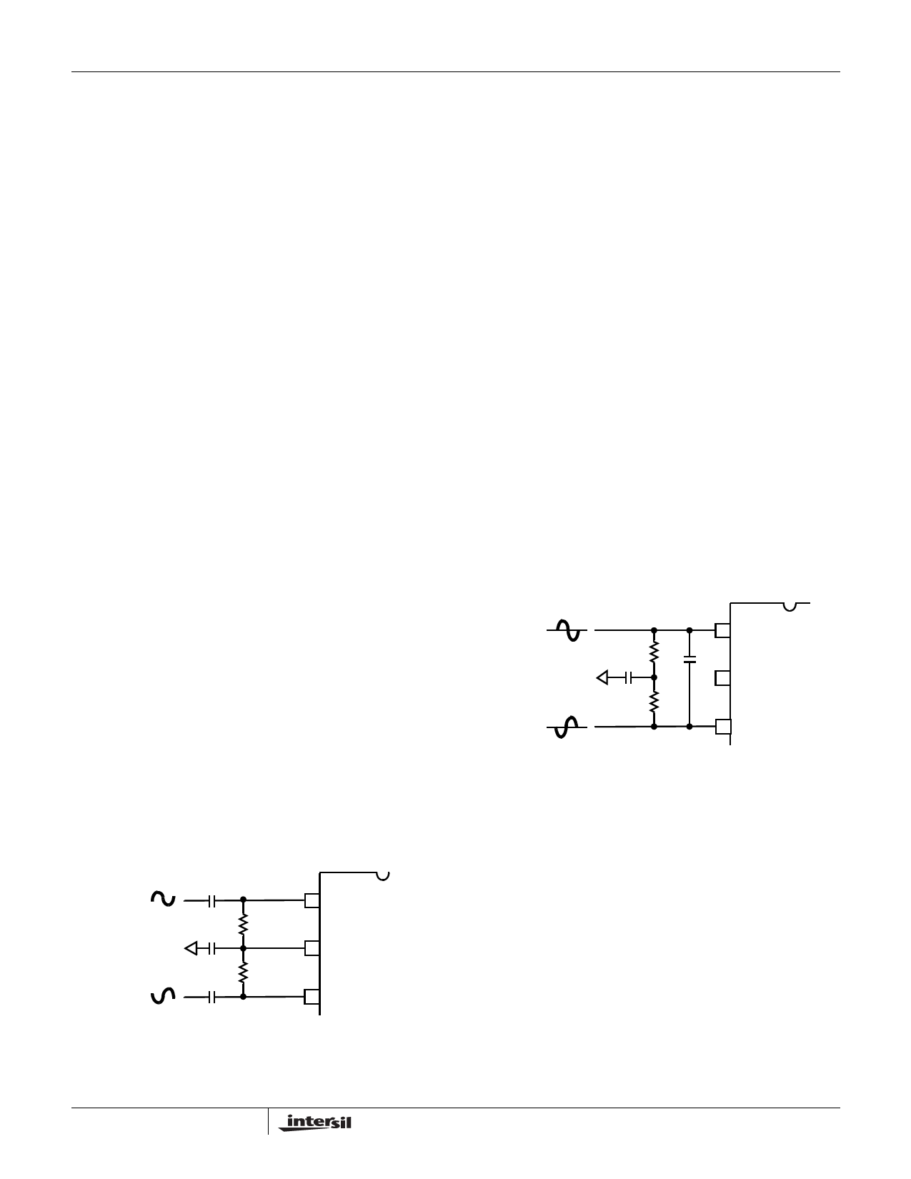
Analog Input, Differential Connection
The analog input to the HI5905 can be configured in various
ways depending on the signal source and the required level
of performance. A fully differential connection (Figure 9) will
give the best performance for the converter.
Since the HI5905 is powered off a single +5V supply, the
analog input must be biased so it lies within the analog input
common mode voltage range of 1.0V to 4.0V. The perfor-
mance of the ADC does not change significantly with the
value of the analog input common mode voltage.
VIN
VIN+
HI5905
VDC
-VIN
VIN-
FIGURE 9. AC COUPLED DIFFERENTIAL INPUT
A 2.3V DC bias voltage source, VDC, half way between the
top and bottom internal reference voltages, is made avail-
able to the user to help simplify circuit design when using a
differential input. This low output impedance voltage source
is not designed to be a reference but makes an excellent
bias source and stays within the analog input common mode
voltage range over temperature.
The difference between the converter’s two internal voltage ref-
erences is 2V. For the AC coupled differential input, (Figure 9), if
VIN is a 2VP-P sinewave with -VIN being 180 degrees out of
phase with VIN, then VIN+ is a 2VP-P sinewave riding on a DC
bias voltage equal to VDC and VIN- is a 2VP-P sinewave riding
on a DC bias voltage equal to VDC. Consequently, the con-
verter will be at positive full scale, resulting in a digital data
output code with D13 (MSB) equal to a logic “0” and D0-D12
equal to logic “1” (see Table 1, A/D Code Table), when the VIN+
input is at VDC+1V and the VIN- input is at VDC-1V
(VIN+ - VIN- = 2V). Conversely, the ADC will be at negative full
scale, resulting in a digital data output code with D13 (MSB)
equal to a logic “1” and D0-D12 equal to logic “0” (see Table 1,
A/D Code Table), when the VIN+ input is equal to VDC-1V and
VIN- is at VDC+1V (VIN+-VIN- = -2V). From this, the converter
is seen to have a peak-to-peak differential analog input voltage
range of 2V.
The analog input can be DC coupled (Figure 10) as long as
the inputs are within the analog input common mode voltage
range (1.0V ≤ VDC ≤ 4.0V).
TABLE 1. A/D CODE TABLE
DIFFERENTIAL
TWO’S COMPLEMENT BINARY OUTPUT CODE
CODE
CENTER
INPUT VOLT-
AGE€ † (USING
MSB
LSB
DESCRIP- INTERNAL
TION
REFERENCE) D13 D12 D11 D10 D9 D8 D7 D6 D5 D4 D3 D2 D1 D0
+Full Scale
(+FS) - 1/4
LSB
+1.99994V
0
1
1
1
1
1
1
1
1
1
1
1
1
1
+FS - 1 1/4 1.99969V
LSB
0
1
1
1
1
1
1
1
1
1
1
1
1
0
+ 3/4 LSB 183.105µV
0
0
0
0
0
0
0
0
0
0
0
0
0
0
- 1/4 LSB -61.035µV
1
1
1
1
1
1
1
1
1
1
1
1
1
1
-FS + 1 3/4 -1.99957V
LSB
1
0
0
0
0
0
0
0
0
0
0
0
0
1
-Full Scale
(-FS) + 3/4
LSB
-1.99982V
1
0
0
0
0
0
0
0
0
0
0
0
0
0
† The voltages listed above represent the ideal center of each two’s complement binary output code shown.
20
Share Link: 