MC145745FW Просмотр технического описания (PDF) - Motorola => Freescale
Номер в каталоге
Компоненты Описание
производитель
MC145745FW Datasheet PDF : 16 Pages
| |||
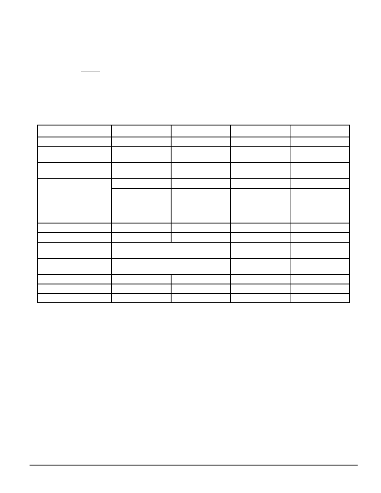
SCP REGISTER MAP
The MC145745 register map is shown in Table 2. Seven of
the 4–bit wide byte registers (BR) are provided in the register
block. According to these published specifications, BR signi-
fies each register and the address of SCP data. R/W is the
read/write register, and RO is read only. If there is a high to
low pulse on the RESET pin or the power supply turns off,
this register returns to the default state.
The default condition that occurs after a power reset is as
follows.
BR0 V.23 Receive, Transmit Enable
BR1 DTMF CDON = 30 ms, DTMF CDOFF = 25 ms
FSK CDON = 450 ms, FSK CDOFF = 30 ms
BR2 FSK Mode
BR3 AGC Range = Maximum,
Carrier Detect Level: High
BR4 Transmission Gain = Maximum
BR5 DTMF Transmission: 941 Hz + 1633 Hz
BR6 DTMF Reception: Unknown
Table 2. SCP Register Map
Register
b3 (Bit 3: MSB)
b2 (Bit 2)
b1 (Bit1)
b0 (Bit 0: LSB)
BR0 (R/W)
Modem Choice
FSK Channel
0 V.23
V.21: Answer
V.23: Receive
1 V.21
V.21: Originate
V.23: Transmit
BR1 (R/W)
FSK CDT2
FSK CDT1
TCDON
b3=0, b2=0 : 450 ms
b3=0, b2=1 : 15 ms
b3=1, b2=0 : 15 ms
b3=1, b2=1 : 75 ms
TCDOFF
b3=0, b2=0 : 30 ms
b3=0, b2=1 : 30 ms
b3=1, b2=0 : 15 ms
b3=1, b2=1 : 10 ms
BR2 (R/W) (see Table 3)
Function Mode 4
Function Mode 3
BR3 (R/W)
AGC Range 2
AGC Range 1
0 B3=0, b2=0 : – 5 to + 20 dB
B3=0, b2=1 : – 5 to + 15 dB
1 b3=1, b2=0 : – 5 to + 10 dB
b3=1, b2=1 : – 5 to + 5 dB
BR4 (R/W) (see Table 4)
Transmission Gain 4
Transmission Gain 3
BR5 (R/W) (see Table 5)
Tone Transmission 4
Tone Transmission 3
BR6 (RO) (see Table 5)
DTMF Reception 4
DTMF Reception 3
NOTES:
1. BR0 (b0) is a non–working bit.
2. DTMF Loopback data is entered into BR5 and output from the parallel port.
Transmission Enable
Enable
Disable
DTMF CDT2
TCDON
b1=0, b0=0 : 30 ms
b1=0, b0=1 : 35 ms
b1=1, b0=0 : 45 ms
DTMF CDT1
TCDOFF
b1=0, b0=0 : 25 ms
b1=0, b0=1 : 35 ms
b1=1, b0=0 : 25 ms
Function Mode 2
Function Mode 1
Carrier Detect Level 1 Test
High Level
(Set when VCC = 5 V)
Low Level
(Set when VCC = 3.6 V)
Transmission Gain 2
Normal
Test Mode
Transmission Gain 1
Tone Transmission 2
Tone Transmission 1
DTMF Reception 2
DTMF Reception 1
MOTOROLA
MC145745
11
Share Link: 