TDA1541A Просмотр технического описания (PDF) - Philips Electronics
Номер в каталоге
Компоненты Описание
производитель
TDA1541A Datasheet PDF : 12 Pages
| |||
Philips Semiconductors
Stereo high performance 16-bit DAC
Product specification
TDA1541A
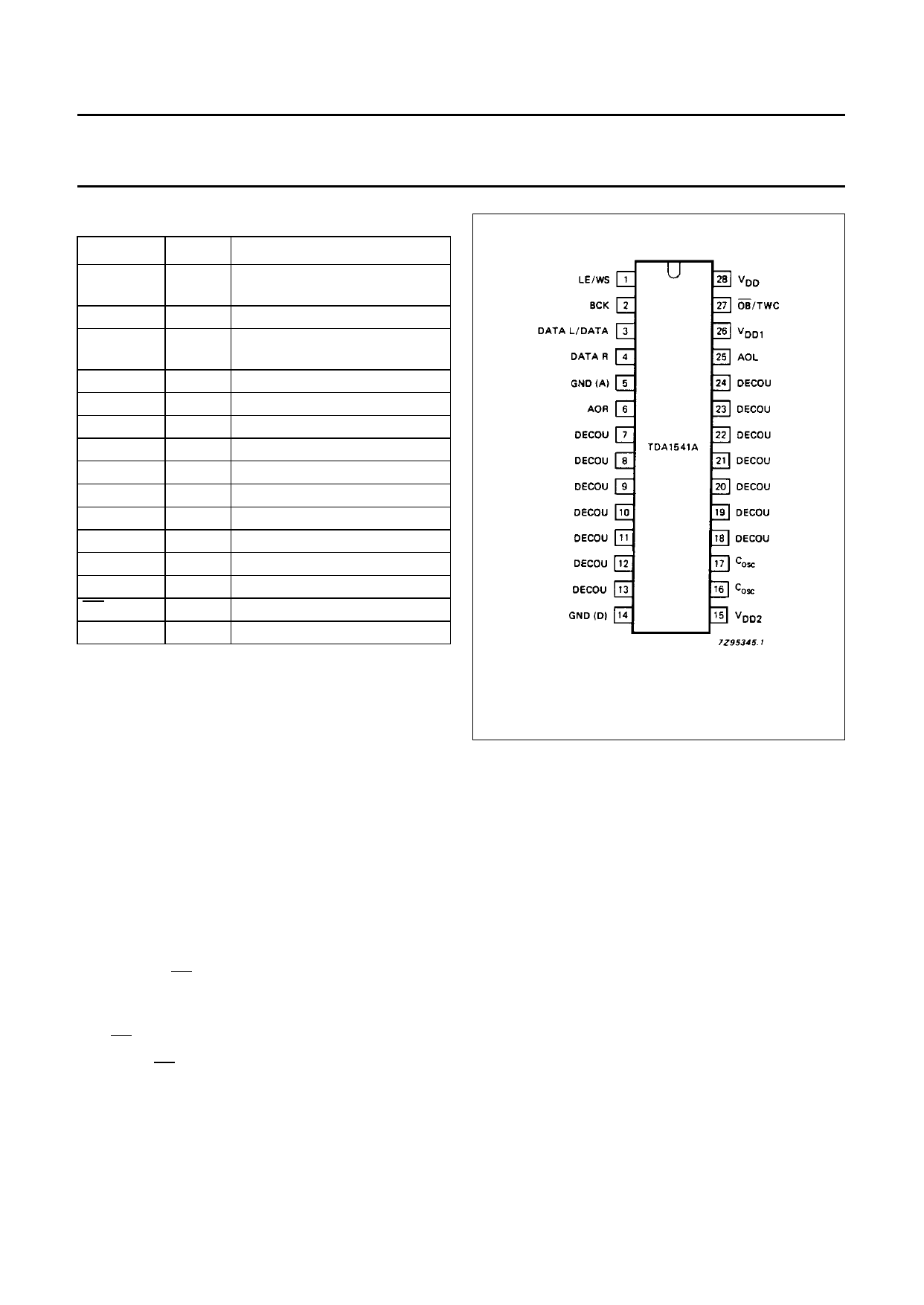
PINNING
SYMBOL
LE/WS(1)
BCK(1)
DATA L
/DATA(1)
DATA R(1)
GND(A)
AOR
DECOU
GND (D)
VDD2
COSC
DECOU
AOL
VDD1
OB/TWC(1)
VDD
PIN
DESCRIPTION
1
latch enable input/ word select
input
2 bit clock input
3
data left channel input/ data
input (selected format)
4 data right channel input
5 analog ground
6 right channel output
7 to 13 decoupling
14 digital ground
15 −15 V supply voltage
16,17 oscillator
18 to 24 decoupling
25 left channel output
26 −5 V supply voltage
27 mode select input
28 +5 V supply voltage
Note
1. See Table 1 data selection input.
Fig.2 Pin configuration
FUNCTIONAL DESCRIPTION
The TDA1541A accepts input sample formats in time multiplexed mode or simultaneous mode up to 16-bit word length.
The most significant bit (MSB) must always be first. The flexible input data format allows easy interfacing with signal
processing chips such as interpolation filters, error correction circuits, pulse code modulation adaptors and audio signal
processors (ASP).
The high maximum input bit-rate and fast setting facilitates application in 8 × oversampling systems
(44.1 kHz to 352.8 kHz or 48 kHz to 384 kHz) with the associated simple analog filtering function (low order, linear phase
filter).
Input data selection (see also Table 1)
With the input OB/TWC connected to ground, data input (offset binary format) must be in time multiplexed mode. It is
accompanied with a word select (WS) and a bit clock input (BCK) signal. The converted samples appear at the output,
at the first positive going transition of the bit clock signal after a negative going transition of the word select signal.
With OB/TWC connected to VDD the mode is the same but the data format must be in the two’s complement.
When input OB/TWC input is connected to VDD1 the two channels of data (L/R) are input simultaneously via DATA L and
DATA R, accompanied with BCK and a latch-enable input (LE). With this mode selected the data must be in offset binary.
The converted samples appear at the output at the positive going transition of the latch enable signal.
The format of the data input signals is shown in Fig.5 and 6.
February 1991
4
Share Link: 