CXD2719Q Просмотр технического описания (PDF) - Sony Semiconductor
Номер в каталоге
Компоненты Описание
производитель
CXD2719Q Datasheet PDF : 59 Pages
| |||
CXD2719Q
1-2. When Pro Logic mode is off
Unless otherwise specified, the measurement conditions are as given below.
• VIN (L, R, C, S) = 2.0Vrms (= 0dB)
• fIN = 1kHz
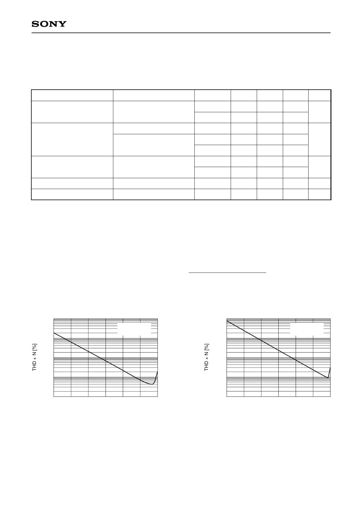
Item
Measurement conditions Channels Min. Typ. Max. Unit
S/N ratio
EIAJ
L, R
(with "A" weighting filter)
C, S
97
dB
90
THD + N∗11
EIAJ (0dB)
EIAJ (–3dB)
(all)
0.03 1.00
L, R
0.004
%
C, S
0.01
Dynamic range∗12
EIAJ (–60dB)
ADC maximum input level∗13
Output level∗14
(Full-scale output)
L, R
93
dB
C, S
83
(all)
1.33
Vrms
(all)
1.7
1.85
2.0 Vrms
∗11 See Graphs 1a and 1b.
∗12 THD + N during –60 dB input
∗13 The analog input level at which the ADC outputs full scale varies according to supply voltage AVDn.
When supply voltage AVDn contains deviation, calculate the maximum input level from (Formula 1) below
and adjust the level with the ADC front-end prefilter, etc., so that the waveform is not clipped at the
minimum voltage.
Minimum supply voltage [V]
ADC maximum input level [Vrms] = 1.33 [Vrms] ×
(Formula 1)
5.0 [V]
∗14 Like the ADC, the DAC conversion gain also varies according to supply voltage AVDn. However, the DAC
has the reverse characteristics of the ADC, so the total gain between the ADC and DAC is constant.
10
10
0dB = 2Vrms
fin = 1kHz
1
0dB = 2Vrms
fin = 1kHz
1
0.1
0.1
0.01
0.01
0.001
–60 –50 –40 –30 –20 –10 0
Analog input level [dB]
Graph 1a. L, R Channel Characteristics
0.001
–60 –50 –40 –30 –20 –10 0
Analog input level [dB]
Graph 1b. C, S Channel Characteristics
–9–
Share Link: 