ADP3810AR-12.6 Просмотр технического описания (PDF) - Analog Devices
Номер в каталоге
Компоненты Описание
производитель
ADP3810AR-12.6 Datasheet PDF : 14 Pages
| |||
ADP3810/ADP3811
veAT
+V'N'
R1
80.61ill
0.1pF
q
'!:L
;1PF
IRF7201
101ill
VREF
VSENSE
VCC
OUT
VREF
ADP3811 vcs
250>2
VCTRL
VCTRL
RC2
560>2
VCTRL &
R2
201ill
0.1pF
GND
CaMP
CC2
220nF
220pF
R8
11ill
~ BATTERY
VREF RTN
11ill
RCI
2000
201ill'
CCI
0.25>2'
1pF
V'N,
RTN
VeAT=2.0V(!!!R+21)
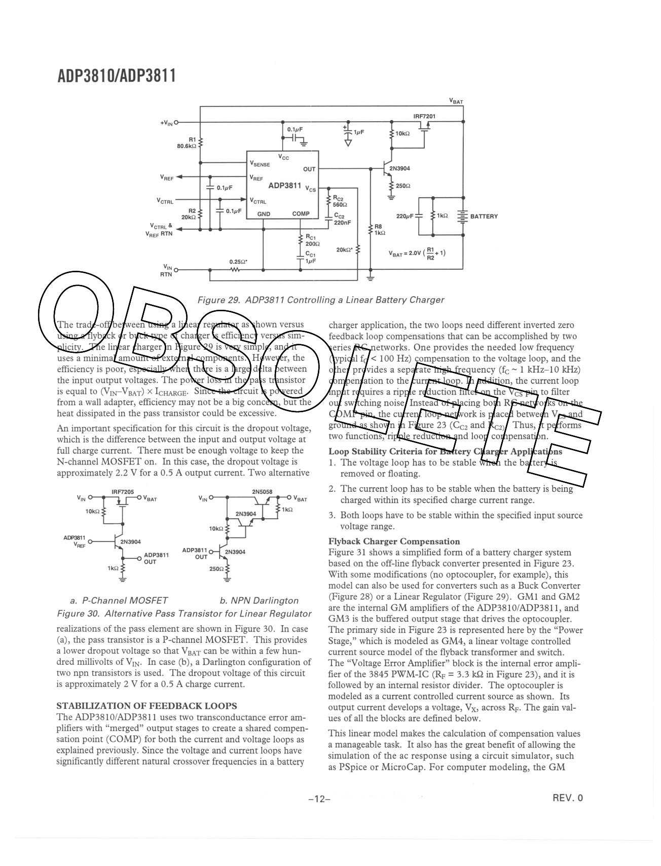
Figure 29. ADP3811 Controlling a Linear Battery Charger
The trade-off between using a linear regulator as shown versus
Ousing a flyback or buck type of charger is efficiency versus sim-
plicity. The linear charger in Figure 29 is very simple, and it
B uses a minimal amount of external components. However, the
S - efficiency is poor, especially when there is a large delta between
the input output voltages. The power loss in the pass transistor
O is equal to (Vrn-VBATx) IeHARGES. ince the circuit is powered
from a wall adapter, efficiency may not be a big concern, but the
L heat dissipated in the pass transistor could be excessive.
E An important specification for this circuit is the dropout voltage,
which is the difference between the input and output voltage at
TE full charge current. There must be enough voltage to keep the
charger application, the two loops need different inverted zero
feedback loop compensations that can be accomplished by two
series RC networks. One provides the needed low frequency
(typical fe < 100 Hz) compensation to the voltage loop, and the
other provides a separate high frequency (fe 1 kHz-10kHz)
compensation to the current loop. In addition, the current loop
input requires a ripple reduction filter on the Ves pin to filter
out switching noise. Instead of placing both RC networks on the
CaMP pin, the current loop network is placed between Ves and
ground as shown in Figure 23 (Cez and Rcz). Thus, it performs
two functions, ripple reduction and loop compensation.
Loop Stability Criteria for Battery Charger Applications
N-channel MOSFET on. In this case, the dropout voltage is
1. The voltage loop has to be stable when the battery is
approximately 2.2 V for a 0.5 A output current. Two alternative
removed or floating.
2N5058
2. The current loop has to be stable when the battery is being
V'N
VeAT
V'N
VeAT
charged within its specified charge current range.
ADP3811
VREF
ADP3811
OUT
ADP3811
OUT
a. P-Channel MOSFET
b. NPN Darlington
Figure 30. Alternative Pass Transistor for Linear Regulator
realizations of the pass element are shown in Figure 30. In case
(a), the pass transistor is a P-channel MOSFET. This provides
a lower dropout voltage so that VBATcan be within a few hun-
dred millivolts of VIN. In case (b), a Darlington configuration of
two npn transistors is used. The dropout voltage of this circuit
is approximately 2 V for a 0.5 A charge current.
STABIUZATION OF FEEDBACK LOOPS
The ADP3810/ADP3811 uses two transconductance error am-
plifiers with "merged" output stages to create a shared compen-
sation point (COMP) for both the current and voltage loops as
explained previously. Since the voltage and current loops have
significantly different natural crossover frequencies in a battery
3. Both loops have to be stable within the specified input source
voltage range.
Flyback Charger Compensation
Figure 31 shows a simplified form of a battery charger system
based on the off-line flyback converter presented in Figure 23.
With some modifications (no optocoupler, for example), this
model can also be used for converters such as a Buck Converter
(Figure 28) or a linear Regulator (Figure 29). GMI and GM2
are the internal GM amplifiers of the ADP3810/ADP3811, and
GM3 is the buffered output stage that drives the optocoupler.
The primary side in Figure 23 is represented here by the "Power
Stage," which is modeled as GM4, a linear voltage controlled
current source model of the flyback transformer and switch.
The "Voltage Error Amplifier" block is the internal error ampli-
= fier of the 3845 PWM-IC (RF 3.3 k.Qin Figure 23), and it is
followed by an internal resistor divider. The optocoupler is
modeled as a current controlled current source as shown. Its
output current develops a voltage, Vx, across RF. The gain val-
ues of all the blocks are defined below.
This linear model makes the calculation of compensation values
a manageable task. It also has the great benefit of allowing the
simulation of the ac response using a circuit simulator, such
as PSpice or MicroCap. For computer modeling, the GM
-12-
REV, 0
Share Link: 