CY7C1024AV33-15BGC Просмотр технического описания (PDF) - Cypress Semiconductor
Номер в каталоге
Компоненты Описание
производитель
CY7C1024AV33-15BGC Datasheet PDF : 11 Pages
| |||
CY7C1024AV33
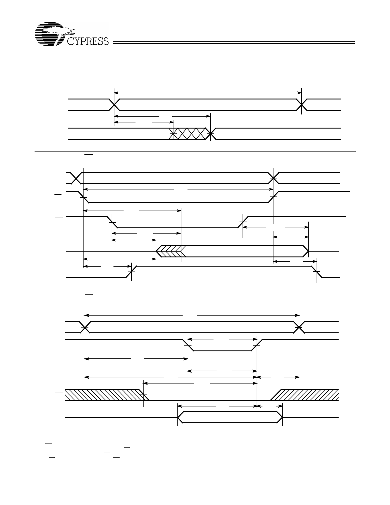
Switching Waveforms
Read Cycle No. 1[10, 11]
tRC
ADDRESS
DATA OUT
tAA
tOHA
PREVIOUS DATA VALID
DATA VALID
Read Cycle No. 2 (OE Controlled)[3, 11, 12]
ADDRESS
CE
OE
DATA OUT
VCC
SUPPLY
CURRENT
tRC
tACE
tDOE
tLZOE
HIGH IMPEDANCE
tLZCE
tPU
50%
DATA VALID
tHZOE
tHZCE
HIGH
IMPEDANCE
tPD
ICC
50%
ISB
Write Cycle No. 1 (CE Controlled)[3, 13, 14]
ADDRESS
CE
tSA
WE
DATA I/O
tWC
tSCE
tSCE
tAW
tPWE
tSD
DATA VALID
tHA
tHD
Notes:
10. Device is continuously selected. OE, CE = VIL.
11. WE is HIGH for read cycle.
12. Address valid prior to or coincident with CE transition LOW.
13. Data I/O is high impedance if OE = VIH.
14. If CE goes HIGH simultaneously with WE going HIGH, the output remains in a high-impedance state.
Document #: 38-05149 Rev. *B
Page 6 of 11
Share Link: 