CDP1823 Просмотр технического описания (PDF) - Intersil
Номер в каталоге
Компоненты Описание
производитель
CDP1823 Datasheet PDF : 7 Pages
| |||
CDP1823, CDP1823C
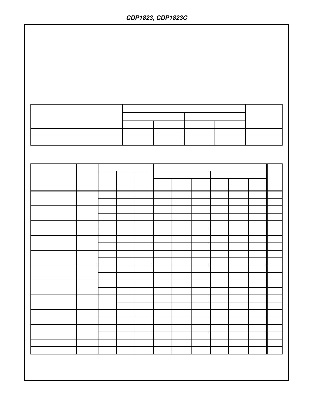
Absolute Maximum Ratings
DC Supply Voltage Range, (VDD)
(All Voltages Referenced to VSS Terminal)
CDP1823 . . . . . . . . . . . . . . . . . . . . . . . . . . . . . . . . -0.5V to +11V
CDP1823C. . . . . . . . . . . . . . . . . . . . . . . . . . . . . . . . -0.5V to +7V
Input Voltage Range, All Inputs . . . . . . . . . . . . . -0.5V to VDD +0.5V
DC Input Current, Any One Input. . . . . . . . . . . . . . . . . . . . . . . . .±10mA
Operating Temperature Range
Package Type D . . . . . . . . .
(TA)
....
.
.
.
.
.
.
.
.
.
.
.
.
-55oC
to
+125oC
Package Type E . . . . . . . . . . . . . . . . . . . . . . . . . . -40oC to +85oC
Thermal Information
Thermal Resistance (Typical)
θJA (oC/W) θJC (oC/W)
PDIP Package . . . . . . . . . . . . . . . . . . .
60
N/A
SBDIP Package . . . . . . . . . . . . . . . . . .
60
17
Maximum Storage Temperature Range (TSTG) . . .-65oC to +150oC
Maximum Junction Temperature
Plastic Package . . . . . . . . . . . . . . . . . . . . . . . . . . . . . . . . . +150oC
Maximum Lead Temperature (During Soldering) . . . . . . . . . . 300oC
Recommended Operating Conditions At TA = Full Package Temperature Range. For maximum reliability, operating conditions
should be selected so that operation is always within the following ranges:
LIMITS
CDP1823D
CDP1823CD
PARAMETER
MIN
MAX
MIN
MAX
UNITS
Supply Voltage Range
4
10.5
4
6.5
V
Recommended Input Voltage Range
VSS
VDD
VSS
VDD
V
Static Electrical Specifications At TA = -40oC to +85oC, Except as Noted:
CONDITIONS
CDP1823
PARAMETER
VO
SYMBOL (V)
VIN
VDD
(NOTE 1)
(V)
(V)
MIN
TYP
Quiescent Device
Current
IDD
-
0, 5
5
-
-
-
0, 10
10
-
-
Output Low (Sink)
Current
IOL
0.4
0, 5
5
2
4
0.5
0, 10
10
4.5
9
Output High (Source)
IOH
4.6
0, 5
5
-1
-2
Current
9.5
0, 10
10
-2.2
-4.4
Output Voltage
Low-Level
VOL
-
0, 5
5
-
0
-
0, 10
10
-
0
Output Voltage
High-Level
VOH
-
0, 5
5
4.9
5
-
0, 10
10
9.9
10
Input Low Voltage
VIL
0.5, 4.5
-
5
-
-
0.5, 9.5
-
10
-
-
Input High Voltage
VIH
0.5, 9.5
-
5
3.5
-
0.5, 9.5
-
10
7
-
Input Leakage Current
IIN
Any
0, 5
5
-
-
Input 0, 10
10
-
-
Operating Current
(Note 2)
IDD1
-
0, 5
5
-
4
-
0, 10
10
-
8
Three-State Output
IOUT
0, 5
0, 5
5
-
-
Leakage Current
0, 10 0, 10
10
-
-
Input Capacitance
CIN
-
-
-
-
5
Output Capacitance
COUT
-
-
-
-
10
NOTES:
1. Typical values are for TA = +25oC and nominal VDD.
2. Outputs open circuited; Cycle time = 1µs.
LIMITS
CDP1823C
MAX
(NOTE 1)
MIN
TYP
MAX
500
-
-
500
1000
-
-
-
-
2
4
-
-
-
-
-
-
-1
-2
-
-
-
-
-
0.1
-
0
0.1
0.1
-
-
-
-
4.9
5
-
-
-
-
-
1.5
-
-
1.5
3
-
-
-
-
3.5
-
-
-
-
-
-
±5
-
-
±5
±10
-
-
-
8
-
4
8
16
-
-
-
±5
-
-
±5
±10
-
-
-
7.5
-
5
7.5
15
-
10
15
UNITS
µA
µA
mA
mA
mA
mA
V
V
V
V
V
V
V
V
µA
µA
mA
mA
µA
µA
pF
pF
6-26
Share Link: 