HT1621 Просмотр технического описания (PDF) - Holtek Semiconductor
Номер в каталоге
Компоненты Описание
производитель
HT1621 Datasheet PDF : 20 Pages
| |||
HT1621
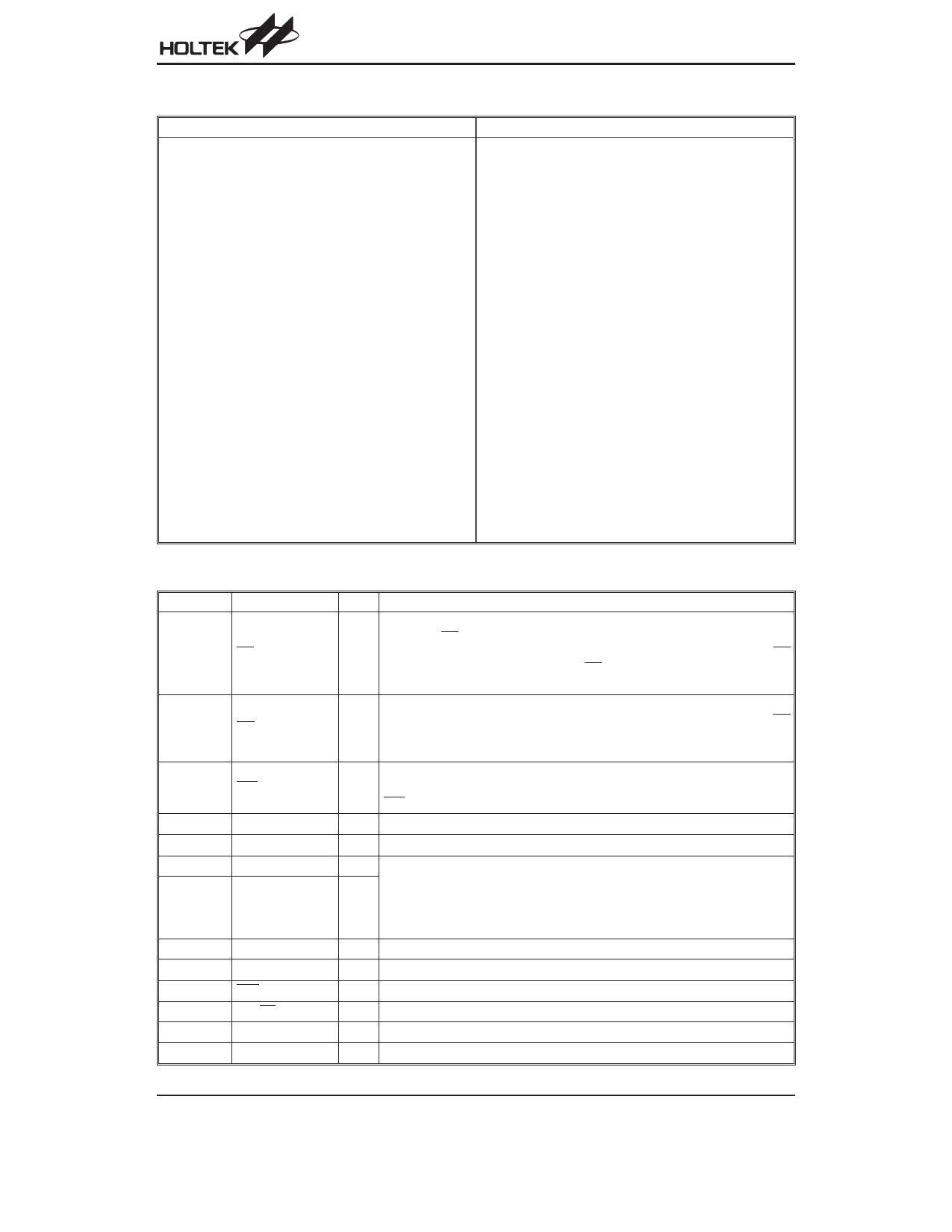
Pad Coordinates
Pad No.
1
2
3
4
5
6
7
8
9
10
11
12
13
14
15
16
17
18
19
20
21
22
23
24
X
-55.04
-58.52
-58.52
-58.52
-58.52
-58.52
-58.52
-58.52
-58.52
-58.52
-44.07
-31.58
-20.70
-13.98
-7.05
-0.34
6.33
12.96
19.59
58.14
58.14
58.14
58.14
58.14
Y
59.46
22.18
15.56
5.36
-4.51
-11.14
-34.76
-41.90
-49.13
-59.08
-59.08
-59.08
-59.08
-59.08
-59.08
-59.08
-59.08
-59.08
-59.08
-58.44
-51.81
-45.18
-38.55
-31.92
Pad No.
25
26
27
28
29
30
31
32
33
34
35
36
37
38
39
40
41
42
43
44
45
46
47
48
X
58.14
58.14
58.14
58.14
58.14
58.14
58.14
58.14
55.55
48.92
42.29
35.66
29.03
22.40
15.77
9.14
2.42
-4.21
-10.84
-17.47
-24.10
-30.73
-38.17
-45.39
Unit: mil
Y
-25.29
-18.66
-11.94
-5.31
1.32
7.95
14.58
21.21
59.46
59.46
59.46
59.46
59.46
59.46
59.46
59.46
59.46
59.46
59.46
59.46
59.46
59.46
59.46
59.46
Pad Description
Pad No.
Pad Name
1
CS
2
RD
3
WR
4
DATA
5
VSS
7
OSCI
6
OSCO
8
9
10
11, 12
13~16
48~17
VLCD
VDD
IRQ
BZ, BZ
COM0~COM3
SEG0~SEG31
I/O
Function
Chip selection input with pull-high resistor
When the CS is logic high, the data and command read from or written to
I the HT1621 are disabled. The serial interface circuit is also reset. But if CS
is at logic low level and is input to the CS pad, the data and command trans-
mission between the host controller and the HT1621 are all enabled.
READ clock input with pull-high resistor
I
Data in the RAM of the HT1621 are clocked out on the falling edge of the RD
signal. The clocked out data will appear on the DATA line. The host control-
ler can use the next rising edge to latch the clocked out data.
WRITE clock input with pull-high resistor
I Data on the DATA line are latched into the HT1621 on the rising edge of the
WR signal.
I/O Serial data input/output with pull-high resistor
¾ Negative power supply, ground
I The OSCI and OSCO pads are connected to a 32.768kHz crystal in order to
generate a system clock. If the system clock comes from an external clock
source, the external clock source should be connected to the OSCI pad. But
O if an on-chip RC oscillator is selected instead, the OSCI and OSCO pads
can be left open.
I LCD power input
¾ Positive power supply
O Time base or WDT overflow flag, NMOS open drain output
O 2kHz or 4kHz tone frequency output pair
O LCD common outputs
O LCD segment outputs
Rev. 1.30
4
August 6, 2003
Share Link: 