MC1489 Просмотр технического описания (PDF) - Motorola => Freescale
Номер в каталоге
Компоненты Описание
производитель
MC1489 Datasheet PDF : 6 Pages
| |||
MC1489, A
APPLICATIONS INFORMATION
General Information
The Electronic Industries Association (EIA) has released
the EIA–232D specification detailing the requirements for the
interface between data processing equipment and data
communications equipment. This standard specifies not only
the number and type of interface leads, but also the voltage
levels to be used. The MC1488 quad driver and its
companion circuit, the MC1489 quad receiver, provide a
complete interface system between DTL or TTL logic levels
and the EIA–232D defined levels. The EIA–232D
requirements as applied to receivers are discussed herein.
The required input impedance is defined as between
3000 Ω and 7000 Ω for input voltages between 3.0 and 25 V
in magnitude; and any voltage on the receiver input in an
open circuit condition must be less than 2.0 V in magnitude.
The MC1489 circuits meet these requirements with a
maximum open circuit voltage of one VBE.
The receiver shall detect a voltage between – 3.0 and
– 25 V as a Logic “1” and inputs between 3.0 and 25 V as a
Logic “0.” On some interchange leads, an open circuit of
power “OFF” condition (300 Ω or more to ground) shall be
decoded as an “OFF” condition or Logic “1.” For this reason,
the input hysteresis thresholds of the MC1489 circuits are all
above ground. Thus an open or grounded input will cause the
same output as a negative or Logic “1” input.
Device Characteristics
The MC1489 interface receivers have internal feedback
from the second stage to the input stage providing input
hysteresis for noise rejection. The MC1489 input has typical
turn–on voltage of 1.25 V and turn–off of 1.0 V for a typical
hysteresis of 250 mV. The MC1489A has typical turn–on of
1.95 V and turn–off of 0.8 V for typically 1.15 V of hysteresis.
Each receiver section has an external response control
node in addition to the input and output pins, thereby allowing
the designer to vary the input threshold voltage levels. A
resistor can be connected between this node and an external
power supply. Figures 2, 4 and 5 illustrate the input threshold
voltage shift possible through this technique.
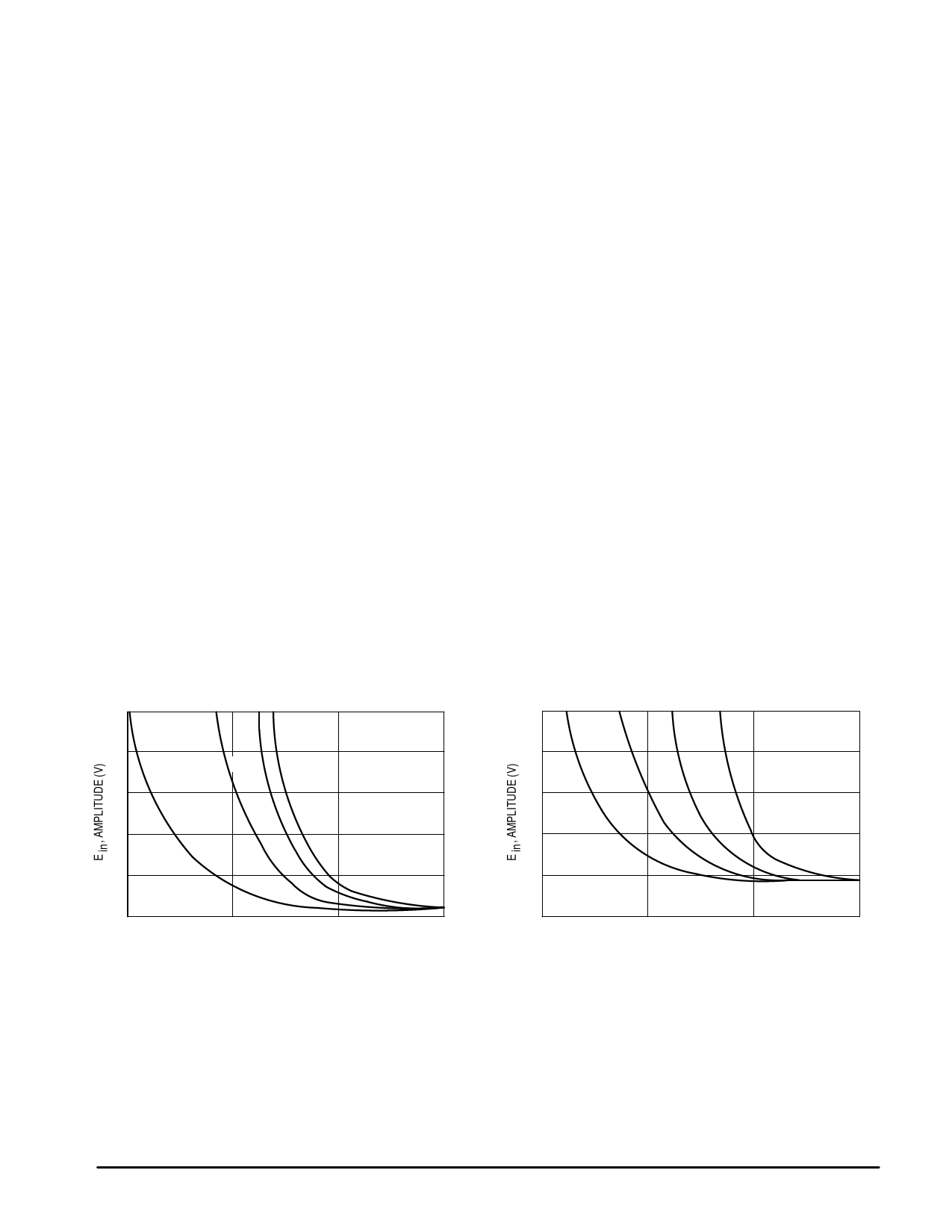
This response node can also be used for the filtering of
high frequency, high energy noise pulses. Figures 8 and 9
show typical noise pulse rejection for external capacitors of
various sizes.
These two operations on the response node can be
combined or used individually for many combinations of
interfacing applications. The MC1489 circuits are particularly
useful for interfacing between MOS circuits and MDTL/MTTL
logic systems. In this application, the input threshold voltages
are adjusted (with the appropriate supply and resistor values)
to fall in the center of the MOS voltage logic levels (see
Figure 10).
The response node may also be used as the receiver input
as long as the designer realizes that he may not drive this
node with a low impedance source to a voltage greater than
one diode above ground or less than one diode below
ground. This feature is demonstrated in Figure 11 where two
receivers are slaved to the same line that must still meet the
EIA–232D impedance requirement.
Figure 8. Typical Turn On Threshold versus
Capacitance from Response Control Pin to GND
6
MC1489
5
10 pF 100 pF 300 pF 500 pF
4
3
2
1
10
100
1000
10,000
PW, INPUT PULSE WIDTH (ns)
Figure 9. Typical Turn On Threshold versus
Capacitance from Response Control Pin to GND
6
MC1489A
5
12 pF 100 pF 300 pF 500 pF
4
3
2
1
10
100
1000
10,000
PW, INPUT PULSE WIDTH (ns)
4
MOTOROLA ANALOG IC DEVICE DATA
Share Link: 