LT1431 Просмотр технического описания (PDF) - Linear Technology
Номер в каталоге
Компоненты Описание
производитель
LT1431 Datasheet PDF : 14 Pages
| |||
LT1431
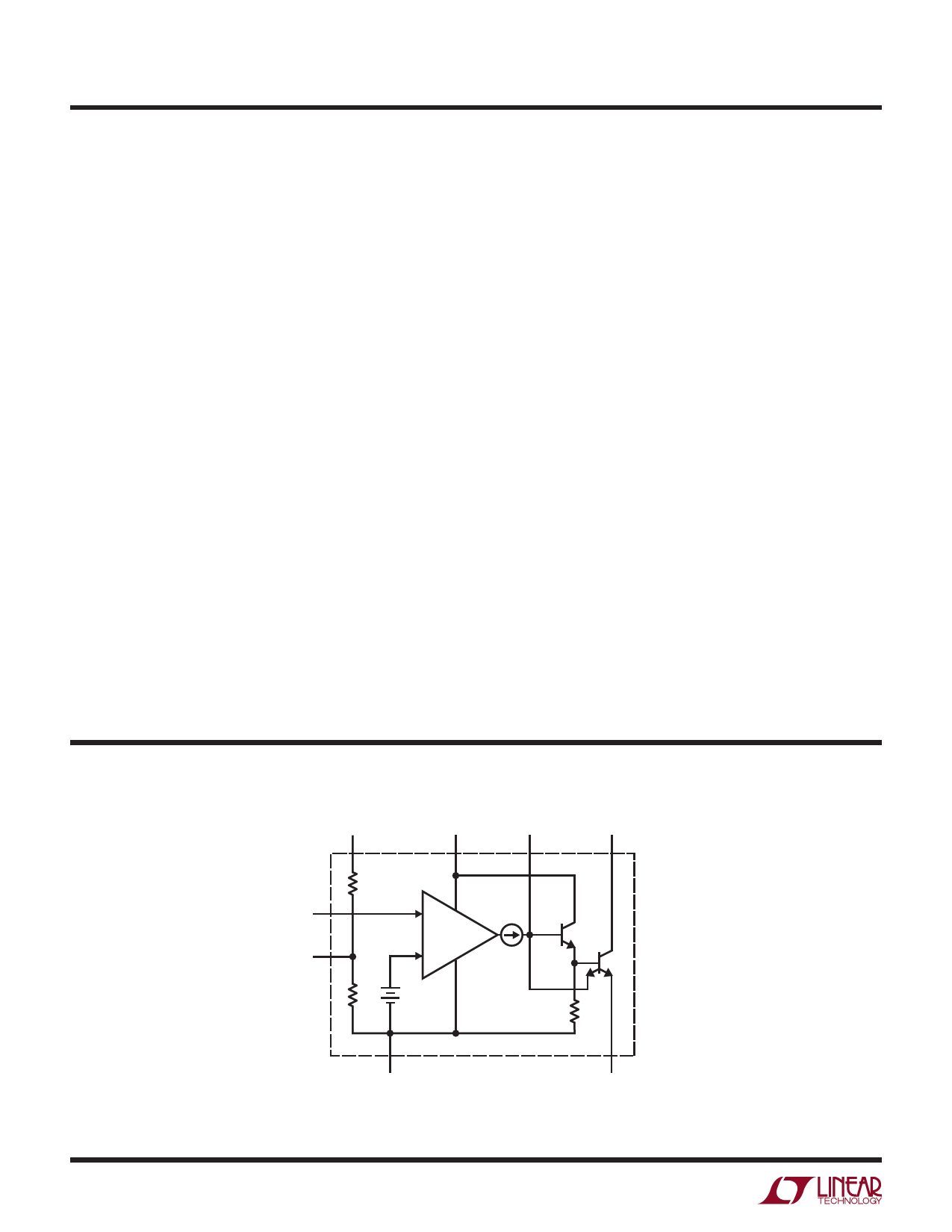
Pin Functions
COLL (Pin 1): Open collector of the output transistor. The
maximum pin voltage is 36V. The saturation voltage at
100mA is approximately 1V.
COMP (Pin 2): Base of the driver for the output transis-
tor. This pin allows additional compensation for complex
feedback systems and shutdown of the regulator. It must
be left open if unused.
V + (Pin 3): Bias voltage for the entire shunt regulator.
The maximum input voltage is 36V and the minimum to
operate is equal to VREF (2.5V). The quiescent current is
typically 0.6mA.
RTOP (Pin 4): Top of the on-chip 5k-5k resistive divider
that guarantees 1% accuracy of operation as a 5V shunt
regulator with no external trim. The pin is tied to COLL for
self-contained 5V operation. It may be left open if unused.
See note on parasitic diodes below.
GND-S (Pin 5): Ground reference for the on-chip resis-
tive divider and shunt regulator circuitry except for the
output transistor. This pin allows external current limit
of the output transistor with one resistor between GND-F
(force) and GND-S (sense).
GND-F (Pin 6): Emitter of the output transistor and sub-
strate connection for the die.
RMID (Pin 7): Middle of the on-chip resistive divider string
between RTOP and GND-S. The pin is tied to REF for self-
contained 5V operation. It may be left open if unused.
REF (Pin 8): Control pin of the shunt regulator with a
2.5V threshold. If V+ > 3V, input bias current cancellation
reduces IB to 0.2µA typical.
COMP, RTOP, RMID, and REF have static discharge protection
circuits that must not be activated on a continuous basis.
Therefore, the absolute maximum DC voltage on these pins
is 6V, well beyond the normal operating conditions.
As with all bipolar ICs, the LT1431 contains parasitic diodes
which must not be forward biased or else anomalous
behavior will result. Pin conditions to be avoided are RTOP
below RMID in voltage and any pin below GND-F in voltage
(except for GND-S).
The following pin definitions apply to the Z package.
CATHODE: Corresponds to COLL and V+ tied together.
ANODE: Corresponds to GND-S and GND-F tied together.
REF: Corresponds to REF.
Block Diagram
RTOP
4
5k
8
REF
7
RMID
5k
V+
3
+
gm =
4mA/V
–
2.5V
COMP
2
COLLECTOR
1
5
GND-SENSE
LT1431 BD
6
GND-FORCE
1431fd
Share Link: 