NCV431A Просмотр технического описания (PDF) - ON Semiconductor
Номер в каталоге
Компоненты Описание
производитель
NCV431A Datasheet PDF : 18 Pages
| |||
TL431A, B Series, NCV431A, B Series, SCV431A
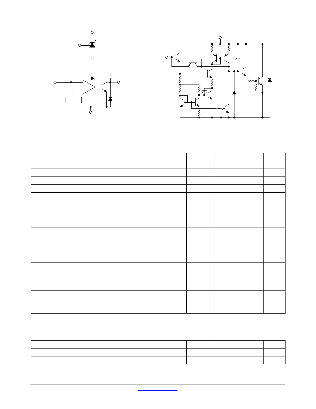
Cathode
(K)
Reference
(R)
Anode
(A)
Figure 1. Symbol
Reference
(R)
Cathode (K)
800
800
20 pF
Reference
(R)
+
-
Cathode
(K)
3.28 k
150
4.0 k
20 pF
2.4 k
7.2 k
10 k
2.5 Vref
1.0 k
Anode (A)
800
Figure 2. Representative Block Diagram
This device contains 12 active transistors.
Anode (A)
Figure 3. Representative Schematic Diagram
Component values are nominal
MAXIMUM RATINGS (Full operating ambient temperature range applies, unless otherwise noted.)
Rating
Symbol
Value
Unit
Cathode to Anode Voltage
VKA
37
V
Cathode Current Range, Continuous
IK
−100 to +150
mA
Reference Input Current Range, Continuous
Iref
−0.05 to +10
mA
Operating Junction Temperature
TJ
150
°C
Operating Ambient Temperature Range
TL431I, TL431AI, TL431BI
TL431C, TL431AC, TL431BC
NCV431AI, NCV431B, TL431BV, SCV431AI
TA
°C
−40 to +85
0 to +70
−40 to +125
Storage Temperature Range
Tstg
−65 to +150
°C
Total Power Dissipation @ TA = 25°C
Derate above 25°C Ambient Temperature
PD
W
D, LP Suffix Plastic Package
0.70
P Suffix Plastic Package
1.10
DM Suffix Plastic Package
0.52
Total Power Dissipation @ TC = 25°C
Derate above 25°C Case Temperature
D, LP Suffix Plastic Package
PD
W
1.5
P Suffix Plastic Package
3.0
ESD Rating (Note 1)
Human Body Model per JEDEC JESD22−A114F
Machine Model per JEDEC JESD22−A115C
Charged Device Model per JEDEC JESD22−C101E
V
HBM
>2000
MM
>200
CDM
>500
Stresses exceeding those listed in the Maximum Ratings table may damage the device. If any of these limits are exceeded, device functionality
should not be assumed, damage may occur and reliability may be affected.
1. This device contains latch−up protection and exceeds ±100 mA per JEDEC standard JESD78.
RECOMMENDED OPERATING CONDITIONS
Condition
Symbol
Min
Max
Unit
Cathode to Anode Voltage
VKA
Vref
36
V
Cathode Current
IK
1.0
100
mA
Functional operation above the stresses listed in the Recommended Operating Ranges is not implied. Extended exposure to stresses beyond
the Recommended Operating Ranges limits may affect device reliability.
www.onsemi.com
2
Share Link: 