STLVD111(2002) Просмотр технического описания (PDF) - STMicroelectronics
Номер в каталоге
Компоненты Описание
производитель
STLVD111 Datasheet PDF : 12 Pages
| |||
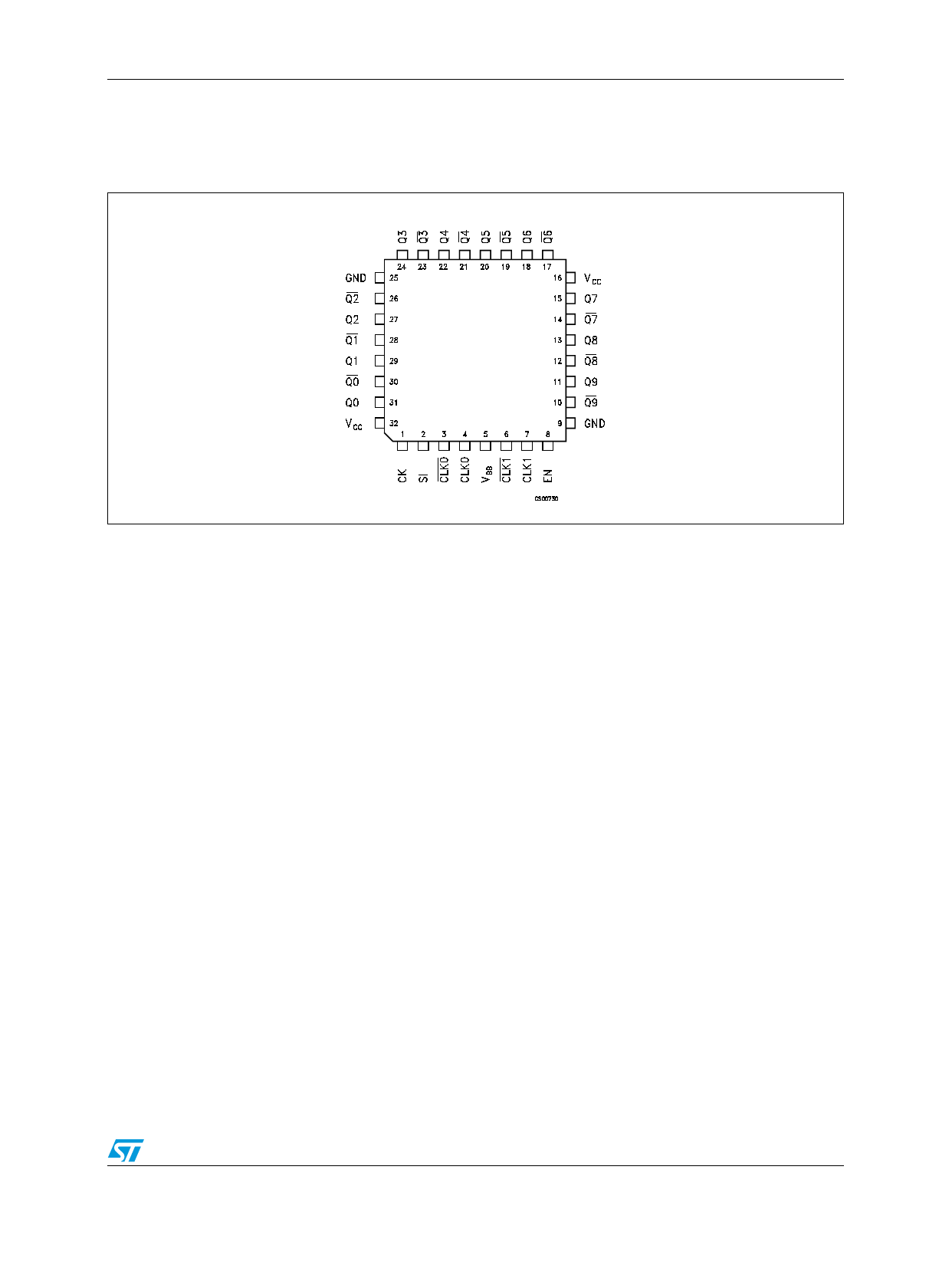
STLVD111
ABSOLUTE MAXIMUM RATINGS
Symbol
Parameter
Value
Unit
VCC Supply Voltage
-0.3 to 2.8
V
VI
Input Voltage
-0.2 to (VCC+0.2)
V
VO
Output Voltage
-0.2 to (VCC+0.2)
V
IOSD Driver Short Circuit Current
Continuous
ESD Electrostatic Discharge (HBM 1.5KΩ, 100pF)
>2
KV
Absolute Maximum Ratings are those values beyond which damage to the device may occur. Functional operation under these condition is
not implied.
THERMAL DATA
Symbol
Parameter
RTj-c Thermal Resistance Junction-Case
Value
13
Unit
°C/W
RECOMMENDED OPERATING CONDITIONS
Symbol
Parameter
VCC Supply Voltage
VIC Receiver Common Mode Input Voltage
TA Operating Free-Air Temperature Range
TJ Operating Junction Temperature
Min
2.375
0.5(VID)
-40
-40
TYP
Max
Unit
2.625
V
2-0.5(VID)
V
85
°C
105
°C
DRIVER ELECTRICAL CHARACTERISTICS (TA = -40 to 85 °C, VCC = 2.5V ± 5%, unless otherwise
specified (Note 1, 2)
Symbol
Parameter
Test Conditions
Value
Unit
Min. Typ. Max.
VOD Output Differential Voltage RL = 100 Ω
(Fig. 2)
400 500 600 mV
∆VOD VOD Magnitude Change
30
mV
VOS Offset Voltage
-40 ≤ TA ≤ 85°C
1.05 1.15 1.25
V
∆VOS VOS Magnitude Change
30
V
IOS Output Short Circuit Current VO = 0V
15
30
mA
VOD = 0V
7
15
NOTE 1: All currents into device pins are positive; all currents out of device pins are negative. All voltages are referenced to device ground
unless otherwise specified.
NOTE 2: All typical values are given for VCC = 2.5V and TA = 25°C unless otherwise stated.
RECEIVER ELECTRICAL CHARACTERISTICS (TA = -40 to 85 °C, VCC = 2.5V ± 5%, unless otherwise
specified (Note 1, 2)
Symbol
Parameter
Test Conditions
Min.
Value
Typ.
Max.
Unit
VIDH
VIDL
IIN
Input Threshold High
Input Threshold Low
Input Current
VI = 0V
VI = 0VCC
-100
42
2
100 mV
mV
100
µA
10
NOTE 1: All currents into device pins are positive; all currents out of device pins are negative. All voltages are referenced to device ground
unless otherwise specified.
NOTE 2: All typical values are given for VCC = 2.5V and TA = 25°C unless otherwise stated.
3/12
Share Link: 