IN74ACT192N Просмотр технического описания (PDF) - Integral Corp.
Номер в каталоге
Компоненты Описание
производитель
IN74ACT192N Datasheet PDF : 7 Pages
| |||
IN74ACT192
PRESETTABLE BCD/DECADE UP/DOWN COUNTER
High-Speed Silicon-Gate CMOS
The IN74ACT192 is identical in pinout to the LS/ALS192,
HC/HCT192. The IN74ACT192 may be used as a level converter
for interfacing TTL or NMOS outputs to High Speed CMOS
inputs.
The counter has two separate clock inputs, a Count Up Clock
and Count Down Clock inputs. The direction of counting is
determined by which input is clocked. The outputs change state
synchronous with the LOW-to-HIGH transitions on the clock
inputs. This counter may be preset by entering the desired data
on the P0, P1, P2, P3 input. When the Parallel Load input is
taken low the data is loaded independently of either clock input.
This feature allows the counters to be used as devide-by-n by
modifying the count lenght with the preset inputs. In addition the
counter can also be cleared. This is accomplished by inputting a
high on the Master Reset input. All 4 internal stages are set to
low independently of either clock input.Both a Terminal Count
Down (TCD) and Terminal Count Up (TCU) Outputs are provided
to enable cascading of both up and down counting functions.
The TCD output produces a negative going pulse when the
counter underflows and TCU outputs a pulse when the
counter overflows. The counter can be cascaded by
connecting the TCU and TCD outputs of one device to the
Count Up Clock and Count Down Clock inputs, respectively,
of the next device.
• TTL/NMOS Compatible Input Levels
• Outputs Directly Interface to CMOS, NMOS, and TTL
• Operating Voltage Range: 4.5 to 5.5 V
• Low Input Current: 1.0 µA; 0.1 µA @ 25°C
• Outputs Source/Sink 24 mA
ORDERING INFORMATION
IN74ACT192N Plastic
IN74ACT192D SOIC
TA = -40° to 85° C for all
packages
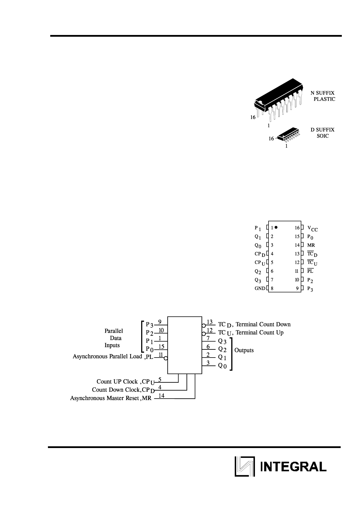
PIN ASSIGNMENT
LOGIC DIAGRAM
PIN 16 =VCC
PIN 8 = GND
1
Share Link: 