MAX362 Просмотр технического описания (PDF) - Maxim Integrated
Номер в каталоге
Компоненты Описание
производитель
MAX362 Datasheet PDF : 10 Pages
| |||
Precision, Quad, SPST Analog Switches
ABSOLUTE MAXIMUM RATINGS
Voltage Referenced to V-
V+ ....................................................................................44V
GND .................................................................................25V
IN_, COM_, NO_, NC_ ...........(V- - 2V) to (V+ + 2V) or 30mA
(whichever occurs first)
Continuous Current (any terminal) .....................................30mA
Peak Current COM, NO, NC
(pulsed at 1ms, 10% duty cycle max)..........................100mA
ESD....................................................................................2000V
Continuous Power Dissipation (TA = +70°C) (Note 1)
Note 1: All leads are soldered or welded to PC board.
Plastic DIP (derate 10.53mW/°C above +70°C)..........842mW
Narrow SO (derate 8.70mW/°C above +70°C)............696mW
Thin QFN (derate 33.3mW/°C above +70°C) ............2667mW
CERDIP (derate 10.00mW/°C above +70°C) ..............800mW
Operating Temperature Ranges:
MAX36_C_ _.......................................................0°C to +70°C
MAX36_E_ _ ....................................................-40°C to +85°C
MAX36_MJE..................................................-55°C to +125°C
Storage Temperature Range ............................-65°C to +150°C
Lead Temperature (soldering, 10s) ................................+300°C
Stresses beyond those listed under “Absolute Maximum Ratings” may cause permanent damage to the device. These are stress ratings only, and
functional operation of the device at these or any other conditions beyond those indicated in the operational sections of the specifications is not implied.
Exposure to absolute maximum rating conditions for extended periods may affect device reliability.
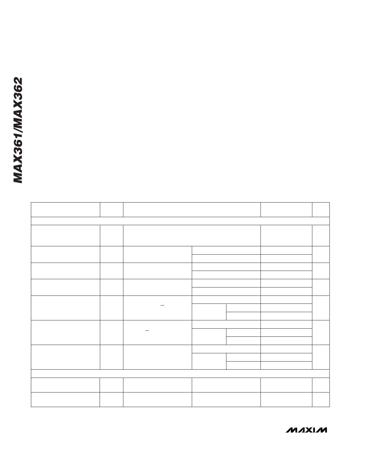
ELECTRICAL CHARACTERISTICS—Dual Supplies
(V+ = 15V, V- = -15V, GND = 0V, VINH = 2.4V, VINL = 0.8V, TA = TMIN to TMAX, unless otherwise noted.)
PARAMETER
SYMBOL
CONDITIONS
ANALOG
Analog-Signal Range
On Resistance
(COM_ to NO_ or
COM_ to NC_ terminals)
On Resistance Match
Between Channels (Note 4)
On Resistance Flatness
(Note 4)
Off Leakage Current
(NO_ or NC_ terminal)
VCOM_,
VNO_,
VNC_
RON
RON
RON
INO_,
INC_
(Note 3)
I(NO or NC) = -10mA,
VCOM_ = 8.5V or -8.5V,
V+ = 13.5V, V- = -13.5V
I(NO or NC) = -10mA,
VCOM_ = 10V or -10V,
V+ = 15V, V- = -15V
I(NO or NC) = -10mA,
VCOM_ = 5V or -5V,
V+ = 15V, V- = -15V
VCOM_ = ±15.5V,
VNC_ or VNO_ = +15.5V,
V+ = 16.5V, V- = -16.5V
Off Leakage Current
(COM_ terminal)
ICOM
VNC_ or VNO_ = ±15.5V,
VCOM_ = +15.5V,
V+ = 16.5V, V- = -16.5V
On Leakage Current
(COM_ and NC_ or NO_
terminal)
DIGITAL
Input Current with
Input Voltage High
Input Current with
Input Voltage Low
ICOM VCOM_ = ±15.5V,
or
VNC_ or VNO_ = ±15.5V,
INO, INC V+ = 16.5V, V- = -16.5V
IINH VIN_ = 2.4V
IINH VIN_ = 0.8V
TA = +25°C
TA = TMIN to TMAX
TA = +25°C
TA = TMIN to TMAX
TA = +25°C
TA = TMIN to TMAX
TA = +25°C
TA = TMAX
C, E
M
TA = +25°C
TA = TMAX
C, E
M
TA = +25°C
TA = TMAX
C, E
M
MIN TYP MAX
(Note 2)
UNITS
-15
15
V
50 85
Ω
100
2
Ω
4
9
Ω
15
-0.50 0.01 0.50
-4
4 nA
-20
20
-0.50 0.01 0.50
-4
4 nA
-20
20
-0.50 0.08 0.50
-6
6 nA
-40
40
-500 0.01 500 nA
-500 0.01 500 nA
2 ________________________________________________________________________________________________
Share Link: 