S24022(2011) Просмотр технического описания (PDF) - Summit Microelectronics
Номер в каталоге
Компоненты Описание
производитель
S24022
(Rev.:2011)
(Rev.:2011)
Summit Microelectronics

S24022 Datasheet PDF : 14 Pages
| |||
S24042/S24043
Read/Write Bit
The last bit of the data stream defines the operation to be
performed. When set to “1,” a read operation is selected;
when set to “0,” a write operation is selected.
While the internal write cycle is in progress, the S24042/
43 inputs are disabled, and the device will not respond to
any requests from the master. Refer to Figure 5 for the
address, ACKnowledge and data transfer sequence.
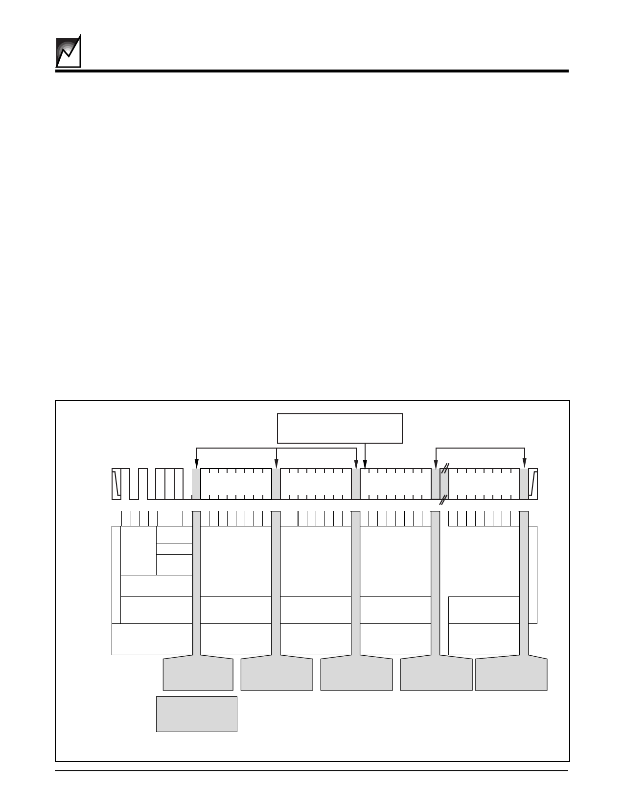
WRITE OPERATIONS
The S24042/43 allows two types of write operations: byte
write and page write. The byte write operation writes a
single byte during the nonvolatile write period (tWR). The
page write operation allows up to 16 bytes in the same
page to be written during tWR.
Byte WRITE
Upon receipt of the slave address and word address, the
S24042/43 responds with an ACKnowledge. After receiv-
ing the next byte of data, it again responds with an
ACKnowledge. The master then terminates the transfer
by generating a STOP condition, at which time the
S24042/43 begins the internal write cycle.
Page WRITE
The S24042/43 is capable of a 16-byte page write opera-
tion. It is initiated in the same manner as the byte-write
operation, but instead of terminating the write cycle after
the first data word, the master can transmit up to 15 more
bytes of data. After the receipt of each byte, the S24042/
43 will respond with an ACKnowledge.
The S24042/43 automatically increments the address for
subsequent data words. After the receipt of each word,
the low order address bits are internally incremented by
one. The high order five bits of the address byte remain
constant. Should the master transmit more than 16 bytes,
prior to generating the STOP condition, the address
counter will “roll over,” and the previously written data will
be overwritten. As with the byte-write operation, all inputs
are disabled during the internal write cycle. Refer to
Figure 5 for the address, ACKnowledge and data transfer
sequence.
Acknowledges Transmitted from
24042/43 to Master Receiver
If single byte-write only,
Stop bit issued here.
Acknowledges Transmitted from
24042/43 to Master Receiver
SDA
Bus
Activity
A
A
X X A R C Word Address C
8WK
K
Data Byte n
A
A
C Data Byte n+1 C
K
K
1010
A
8
0
AAAAAAAA
76543210
DDDDDDDD
76543210
DDDDDDDD
76543210
S
T Device
A Type
R
T
Address Read/Write
0= Write
A
Data Byte n+15 C
K
DDDDDDDD
76543210
S
T
O
P
Slave Address
Master Sends Read
Request to Slave
Master Writes Word
Address to Slave
Master Writes
Data to Slave
Master Writes
Data to Slave
Master Writes
Data to Slave
Master Transmitter
to
Slave Receiver
Master Transmitter
to
Slave Receiver
Master Transmitter
to
Slave Receiver
Master Transmitter
to
Slave Receiver
Master Transmitter
to
Slave Receiver
Slave Transmitter
to
Master Receiver
Slave Transmitter
to
Master Receiver
Slave Transmitter
to
Master Receiver
Slave Transmitter
to
Master Receiver
Slave Transmitter
to
Master Receiver
Shading Denotes
24042/43
SDA Output Active
2011 ILL8 1.0
2011 2.1 8/2/00
FIGURE 5. PAGE/BYTE WRITE MODE
5
SUMMIT MICROELECTRONICS, Inc.
Share Link: