SG7818AIG Просмотр технического описания (PDF) - Microsemi Corporation
Номер в каталоге
Компоненты Описание
производитель
SG7818AIG Datasheet PDF : 7 Pages
| |||
SG7800A/SG7800 SERIES
POSITIVE REGULATOR
ABSOLUTE MAXIMUM RATINGS (Note 1)
Device
Output Voltage
5V
12V
15V
Input Voltage
35V
35V
35V
Input Voltage
(transient) (Note 3)
50V
50V
50V
Input Voltage Differential
(Output shorted to ground)
35V
35V
35V
Operating Junction Temperature
Hermetic (K, T, IG & L - Packages) ......................... 150°C
Note 1. Values beyond which damage may occur.
THERMAL DATA
K Package:
Thermal Resistance-Junction to Case, θJC ................. 3.0°C/W
Thermal Resistance-Junction to Ambient, θJA ............... 35°C/W
T Package:
Thermal Resistance-Junction to Case, θJC .................. 15°C/W
Thermal Resistance-Junction to Ambient, θJA ............ 120°C/W
IG Package:
Thermal Resistance-Junction to Case, θJC ................. 3.5°C/W
Thermal Resistance-Junction to Ambient, θJA .............. 42°C/W
L Package:
Thermal Resistance-Junction to Case, θJC .................. 35°C/W
Thermal Resistance-Junction to Ambient, θJA ............ 120°C/W
Storage Temperature Range .......................... -65°C to 150°C
Lead Temperature (Soldering, 10 Seconds) ................. 300°C
Note A. Junction Temperature Calculation: TJ = TA + (PD x θJA).
Note B. The above numbers forθJC are maximums for the limiting thermal
resistance of the package in a standard mounting configuration.
The θJA numbers are meant to be guidelines for the thermal
performance of the device/pc-board system. All of the above
assume no ambient airflow.
RECOMMENDED OPERATING CONDITIONS (Note 2)
Operating Junction Temperature Range:
SG7800A/SG7800 ........................................ -55°C to 150°C
Note 2. Range over which the device is functional.
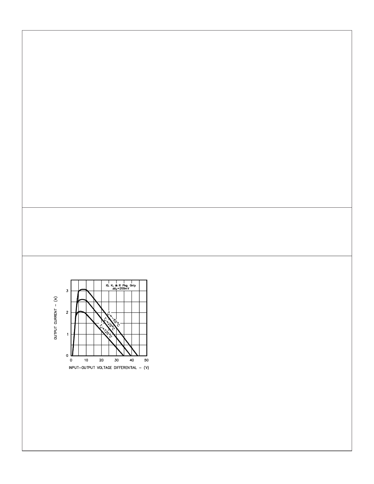
CHARACTERISTIC CURVES
Note 3. Operation at high input voltages is dependent upon load current. When
load current is less than 5mA, output will rise out of regulation as input-
oiutput differential icreases beyond 30V. Note also from Figure 1, that
maximum load current is reduced at high voltages. The 50V input rating
of the SG140A series refers to ability to withstnd high line or transient
conditions without damage. Since the regulator's maximum current
capability is reduced, the output may fall out of regulation at high input
voltages under nominal loading.
FIGURE 1.
PEAK OUTPUT CURRENT
VS. INPUT - OUTPUT DIFFERENTIAL
05/01 Rev 1.4
Copyright © 1997
LINFINITY Microelectronics Inc.
2
11861 Western Avenue ∞ Garden Grove, CA 92841
(714) 898-8121 ∞ FAX: (714) 893-2570
Share Link: 