LTC1412 Просмотр технического описания (PDF) - Linear Technology
Номер в каталоге
Компоненты Описание
производитель
LTC1412 Datasheet PDF : 16 Pages
| |||
LTC1412
WU
TI I G CHARACTERISTICS (Note 5)
SYMBOL
fSAMPLE(MAX)
tTHROUGHPUT
tCONV
tACQ
t1
t2
t3
PARAMETER
Maximum Sampling Frequency
Throughput Time (Acquisition + Conversion)
Conversion Time
Acquisition Time
CS↓ to CONVST↓ Setup Time
CONVST Low Time
CONVST to BUSY Delay
CONDITIONS
(Notes 9, 10)
(Note 10)
CL = 25pF
t4
Data Ready Before BUSY↑
t5
Delay Between Conversions
t6
Data Access Time After CS↓
(Note 10)
CL = 25pF
t7
Bus Relinquish Time
LTC1412C
LTC1412I
t8
CONVST High Time
t9
Aperture Delay of Sample-and-Hold
MIN TYP MAX UNITS
q3
MHz
q
333
ns
q
240
283
ns
q
20
50
ns
q5
ns
q 20
ns
5
ns
q
20
ns
– 20
0
20
ns
q – 25
25
ns
q 50
ns
10
35
ns
q
45
ns
8
30
ns
q
35
ns
q
40
ns
q 20
ns
–1
ns
The q denotes specifications which apply over the full operating
temperature range; all other limits and typicals TA = 25°C.
Note 1: Absolute Maximum Ratings are those values beyond which the life
of a device may be impaired.
Note 2: All voltage values are with respect to ground with DGND and
AGND wired together (unless otherwise noted).
Note 3: When these pin voltages are taken below VSS or above VDD, they
will be clamped by internal diodes. This product can handle input currents
greater than 100mA below VSS or above VDD without latchup.
Note 4: When these pin voltages are taken below VSS they will be clamped
by internal diodes. This product can handle input currents greater than
100mA below VSS without latchup. These pins are not clamped to VDD.
Note 5: VDD = 5V, fSAMPLE = 3MHz and tr = tf = 5ns unless otherwise
specified.
Note 6: Linearity, offset and full-scale specifications apply for a single-
ended AIN input with AIN– grounded.
Note 7: Integral nonlinearity is defined as the deviation of a code from a
straight line passing through the actual endpoints of the transfer curve.
The deviation is measured from the center of the quantization band.
Note 8: Bipolar offset is the offset voltage measured from – 0.5LSB
when the output code flickers between 0000 0000 0000 and
1111 1111 1111.
Note 9: Guaranteed by design, not subject to test.
Note 10: Recommended operating conditions.
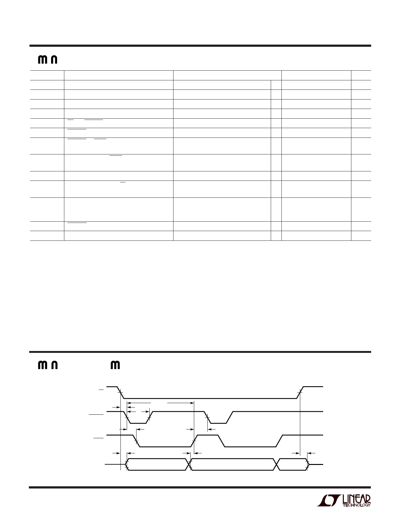
WU
W
TI I G DIAGRA
CS
t1
CONVST
tCONV
t2
t3
t5
BUSY
t6
t4
DATA
DATA (N – 1)
DB11 TO DB0
DATA N
DB11 TO DB0
t7
DATA (N + 1)
DB11 TO DB0
1412 TD
4
Share Link: 