HI5800JCD(1999) Просмотр технического описания (PDF) - Intersil
Номер в каталоге
Компоненты Описание
производитель
HI5800JCD Datasheet PDF : 15 Pages
| |||
HI5800
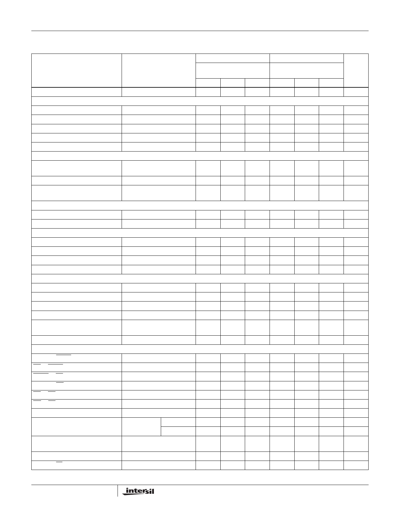
Electrical Specifications AVCC = +5V, DVCC = +5V, AVEE = -5V, DVEE = -5V; Internal Reference Used,
Unless Otherwise Specified (Continued)
HI5800JCD
0oC TO 70oC
HI5800KCD, HI5800BID
0oC TO 70oC
-40oC TO 85oC
PARAMETER
Aperture Jitter, tAJ
ANALOG INPUT
Input Voltage Range
Input Resistance
TEST CONDITIONS
(Note 3)
MIN
TYP
MAX
MIN
TYP
MAX
-
10
20
-
10
20
-
±2.5
±2.7
-
±2.5
±2.7
1
3
-
1
3
-
Input Capacitance
Input Current
Input Bandwidth
-
5
-
-
5
-
-
±1
±10
-
±1
±10
-
20
-
-
20
-
INTERNAL VOLTAGE REFERENCE
Reference Output Voltage,
REFOUT (Loaded)
Reference Output Current
Reference Temperature
Coefficient
(Note 5)
2.450 2.500 2.550 2.470 2.500 2.530
2
-
-
-
20
-
2
-
-
-
13
-
REFERENCE INPUT
Reference Input Range
-
2.5
2.6
-
2.5
2.6
Reference Input Resistance
DIGITAL INPUTS
Input Logic High Voltage, VIH
Input Logic Low Voltage, VIL
Input Logic Current, IIL
Digital Input Capacitance, CIN
DIGITAL OUTPUTS
Output Logic High Voltage, VOH
Output Logic Low Voltage, VOL
Output Logic High Current, IOH
Output Logic Low Current, IOL
Output Three-State Leakage
Current, IOZ
Digital Output Capacitance, COUT
TIMING CHARACTERISTICS
(Note 6)
VIN = 0V, 5V
VIN = 0V
IOUT = -160µA
IOUT = 3.2mA
VOUT = 0V, 5V
-
200
-
-
200
-
2.0
-
-
2.0
-
-
-
-
0.8
-
-
0.8
-
±1
±10
-
±1
±10
-
5
-
-
5
-
2.4
4.3
-
2.4
4.3
-
-
0.22
0.4
-
0.22
0.4
-0.160
-6
-
-0.160
-6
-
3.2
6
-
3.2
6
-
-
±1
±10
-
±1
±10
-
10
-
-
10
-
Minimum CONV Pulse, t1
(Notes 3, 4)
10
-
-
10
-
-
CS to CONV Setup Time, t2
(Note 3)
10
-
-
10
-
-
CONV to CS Setup Time, t3
(Note 3)
0
-
-
0
-
-
Minimum OE Pulse, t4
(Notes 3, 5)
15
-
-
15
-
-
CS to OE Setup Time, t5
(Note 3)
0
-
-
0
-
-
OE to CS Setup Time, t6
(Note 3)
0
-
-
0
-
-
IRQ Delay from Start Convert, t7
(Note 3)
10
20
25
10
20
25
IRQ Pulse Width, t8
JCD, KCD
190
200
230
190
200
230
BID
-
-
-
180
195
230
Minimum Cycle Time for
Conversion, t9
IRQ to Data Valid Delay, t10
Minimum A0 Pulse, t11
(Note 3)
(Notes 3, 5)
-
325
333
-
325
333
-5
0
+5
-5
0
+5
10
-
-
10
-
-
UNITS
ps
V
MΩ
pF
µA
MHz
V
mA
ppm / oC
V
Ω
V
V
µA
pF
V
V
mA
mA
µA
pF
ns
ns
ns
ns
ns
ns
ns
ns
ns
ns
ns
ns
4
Share Link: 