SPT7920 Просмотр технического описания (PDF) - Signal Processing Technologies
Номер в каталоге
Компоненты Описание
производитель
SPT7920 Datasheet PDF : 11 Pages
| |||

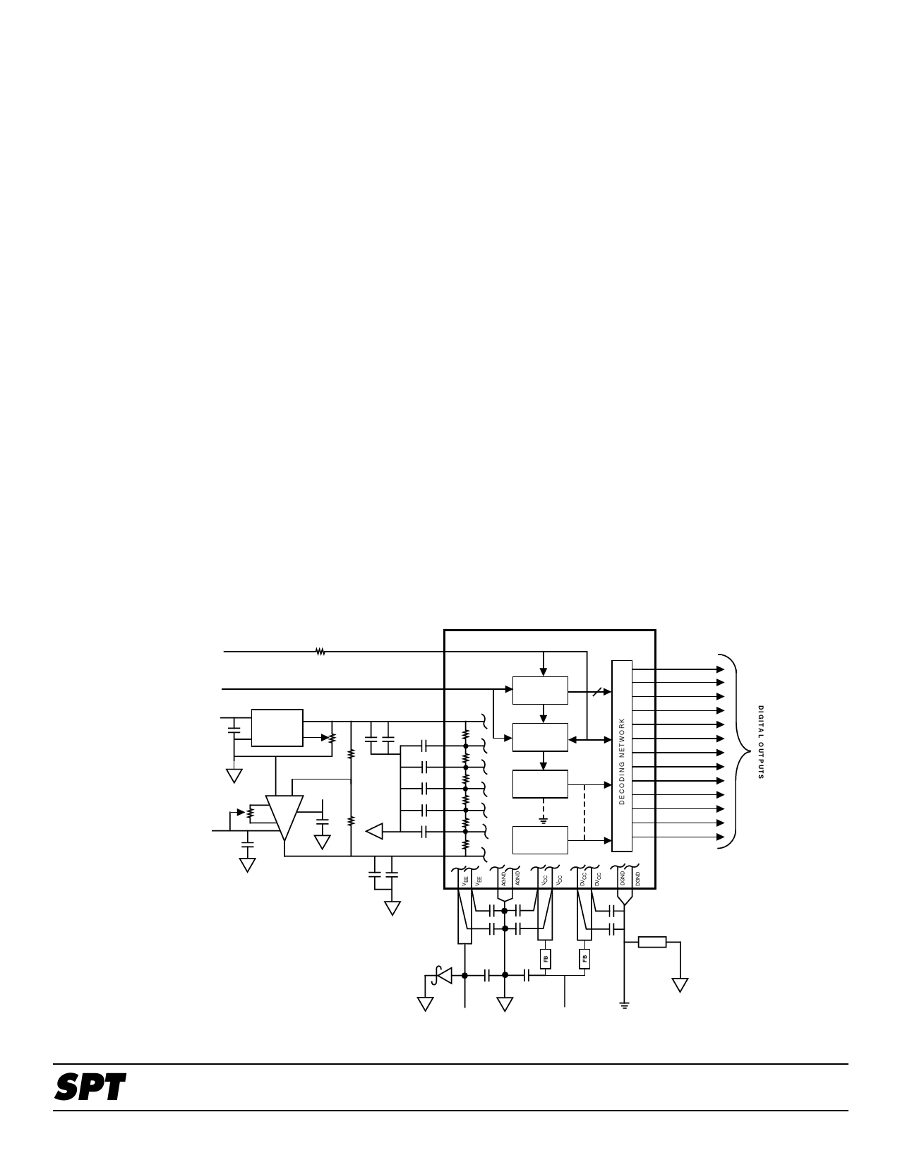
TYPICAL INTERFACE CIRCUIT
The SPT7920 requires few external components to achieve
the stated operation and performance. Figure 2 shows the
typical interface requirements when using the SPT7920 in
normal circuit operation. The following section provides a
description of the pin functions and outlines critical perfor-
mance criteria to consider for achieving the optimal device
performance.
POWER SUPPLIES AND GROUNDING
The SPT7920 requires -5.2 V and +5 V analog supply
voltages. The +5 V supply is common to analog VCC and
digital DVCC. A ferrite bead in series with each supply line is
intended to reduce the transient noise injected into the
analog VCC. These beads should be connected as closely as
possible to the device. The connection between the beads
and the SPT7920 should not be shared with any other
device. Each power supply pin should be bypassed as
closely as possible to the device. Use 0.1 µF for VEE and
VCC, and 0.01 µF for DVCC (chip caps are preferred).
AGND and DGND are the two grounds available on the
SPT7920. These two internal grounds are isolated on the
device. The use of ground planes is recommended to achieve
optimum device performance. DGND is needed for the DVCC
return path (40 mA typical) and for the return path for all digital
output logic interfaces. AGND and DGND should be sepa-
rated from each other and connected together only at the
device through a ferrite bead.
Figure 2 - Typical Interface Circuit
A Schottky or hot carrier diode connected between AGND
and VEE is required. The use of separate power supplies
between VCC and DVCC is not recommended due to potential
power supply sequencing latch-up conditions. Using the
recommended interface circuit shown in figure 2 will provide
optimum device performance for the SPT7920.
VOLTAGE REFERENCE
The SPT7920 requires the use of two voltage references: VFT
and VFB. VFT is the force for the top of the voltage reference
ladder (+2.5 V typ), VFB (-2.5 V typ) is the force for the bottom
of the voltage reference ladder. Both voltages are applied
across an internal reference ladder resistance of 800 ohms.
The +2.5 V voltage source for reference VFT must be current
limited to 20 mA maximum if a different driving circuit is used
in place of the recommended reference circuit shown in figures
2 and 3. In addition, there are five reference ladder taps (VST,
VRT1, VRT2, VRT3, and VSB). VST is the sense for the top of
the reference ladder (+2.0 V), VRT2 is the midpoint of the
ladder (0.0 V typ) and VSB is the sense for the bottom of the
reference ladder (-2.0 V). VRT1 and VRT3 are quarter point
ladder taps (+1.0 and -1.0 V typical, respectively). The
voltages seen at VST and VSB are the true full scale input
voltages of the device when VFT and VFB are driven to the
recommended voltages (+2.5 V and -2.5 V typical respec-
tively). VST and VSB should be used to monitor the actual full
scale input voltage of the device. VRT1, VRT2 and VRT3
should not be driven to the expected ideal values as is
commonly done with standard flash converters. When not
being used, a decoupling capacitor of .01 µF connected to
AGND from each tap is recommended to minimize high
frequency noise injection.
CLK
(TTL)
R1
100 Ω
VIN
(±2 V)
± 2.5 V Max
+5V
C19
1 µF
+
2
VIN
IC1 VOUT 6
(REF-03)
4
GND
Trim
5
+
10 kΩ
1 µF
30 kΩ
+5 V
1
10 kΩ
3
2
+-
IC2
OP-07
8
7
C18
6
.01 µF
- 5.2 V
4
C17
.01 µF
30 kΩ
C16
1 µF
+
+2.5 V
C1
.01 µF C2
.01 µF
C3
.01 µF
C4
.01 µF
C5
.01 µF
C6
.01 µF
-2.5 V
C7
.01 µF
Notes to prevent latch-up due to power sequencing:
1) D1 = Schottky or hot carrier diode, P/N IN5817.
2) FB = Ferrite bead, Fair Rite P/N 2743001111
to be mounted as close to the device as possible. The ferrite bead to the ADC
connection should not be shared with any other device.
3) C1-C13 = Chip cap (recommended) mounted as close to the device's pin as
possible.
4) Use of a separate supply for V CC and DVCC is not recommended.
5) R1 provides current limiting to 45 mA.
6) C8, C9, C10 and C11 should be ten times larger than C12 and C13.
7) C10 = C11 = 0.1 µF cap in parallel with a 4.7 µF cap.
17 CLK
24 VIN
21 VFT
22 VST
R
23 VRT3
2R
25 VRT2
2R
2R
26 VRT1
2R
27 VSB
R
28 VFB
COARSE
4
A/D
ANALOG
PRESCALER
SUCCESSIVE
INTERPOLATION
STAGE # 1
SUCCESSIVE
INTERPOLATION
STAGE # N
D12 14 (OVERRANGE)
D11 13
(MSB)
D10 12
D9 11
D8 10
D7 9
D6 8
D5 7
D4 6
D3 5
D2 4
D1 3
D0 2
(LSB)
18 31
19 30
C8
.1 µF
C9
.1 µF
20 29
C10
C11
16 32
1 15
C12
.01 µF
C13
.01 µF
FB
D1
C15
10 µF
C14
10 µF
+
+
-5.2 V
(Analog)
AGND
+5 V
(Analog)
DGND
SPT
7
SPT7920
3/10/97