SN74S1051T Просмотр технического описания (PDF) - California Micro Devices Corp
Номер в каталоге
Компоненты Описание
производитель
SN74S1051T Datasheet PDF : 2 Pages
| |||
CALIFORNIA MICRO DEVICES
SN 74S1051
ABSOLUTE MAXIMUM RATINGS
Parameter
Supply Voltage
Channel clamp current (continuous)
Operating Temperature
Storage Temperature
Package Power Rating
STANDARD SPECIFICATIONS
Symbol
VDD
I clamp
Tstg
Rating
-0.3V to +7V
±50mA
0OC to 70OC
-65OC to +150OC
625mW, max.
The absolute maximum ratings are limiting values, to be applied individually, beyond which the device may be permanently damaged. Functional
operation under any of these conditions is not guaranteed. Exposing the device to its absolute maximum rating may
affect its reliability.
DIODE CHARACTERISTICS (TA = 0O to 70OC)
Parameter
Conditions
Min
Diode foward voltage
To VDD
IF = 16 mA
IF = 50 mA
0.55V
From GND
IF = 16 mA
IF = 50 mA
0.50V
Reverse Recovery Time (See Note 1) IF = 50mA (estimated)
Channel leakage
0 ≤ VIN ≤ VDD
Input Capacitance
f = 1 MHz, VIN = 2.5V, TA = 25OC, VDD = 5.0V
ESD Protection
MIL-STD-883, Method 3015
4KV
Typ
0.55V
0.70V
0.50V
0.65V
0.1µA
5pF
Max
0.70V
0.90V
0.65V
0.85V
<400pS
5µA
STANDARD PART ORDERING INFORMATION
Package
Ordering Part Number
Pins
Style
Tubes
Tape & Reel
16
SOIC Narrow
SN 74S1051/T
SN 74S1051/R
Part Marking
SN 74S1051
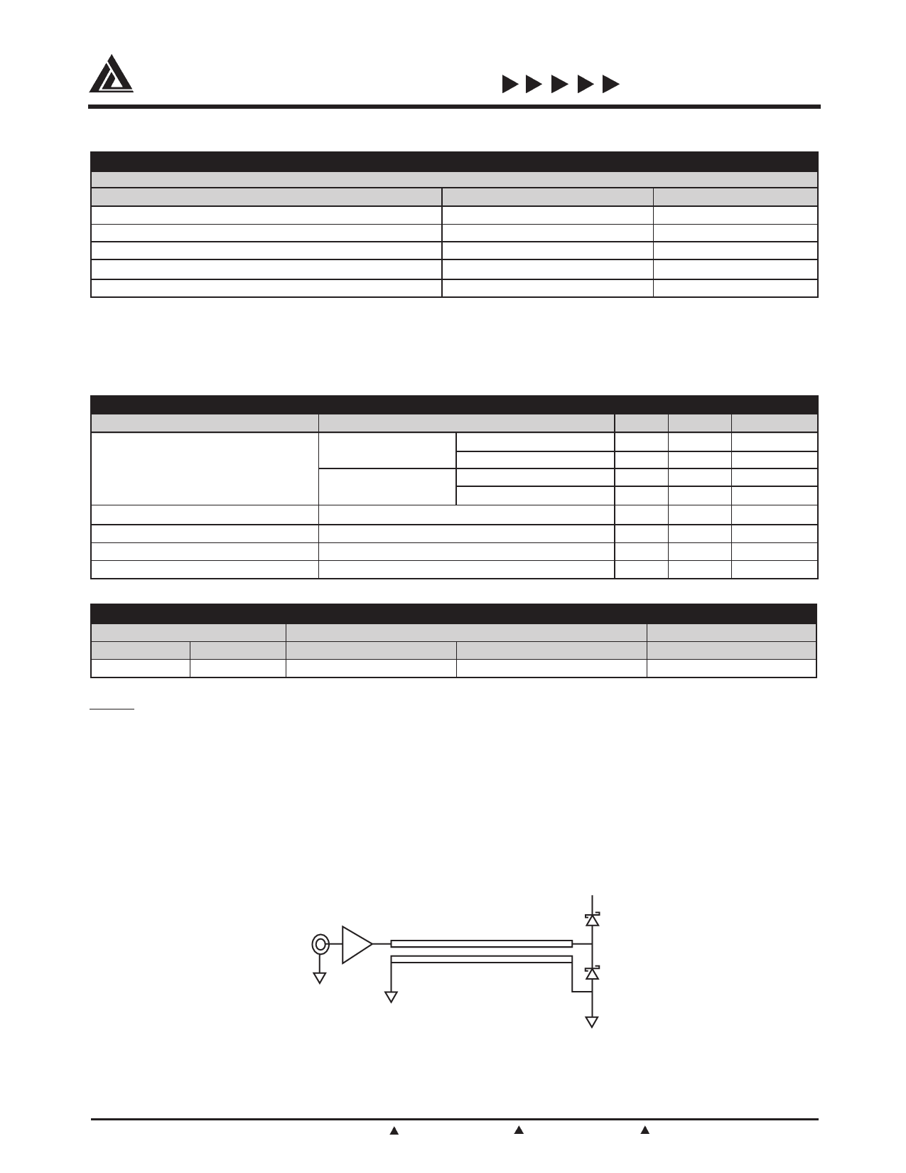
Note 1:
The test circuit depicts the Schottky diodes in their typical application. The impact of a reverse recovery time is measured
using a narrow pulse with 670- pS rise and fall times. This pulse propagates down a 60 cm, 54 ohm strip line fabricated
on a multi-layer, controlled impedance printed circuit board. In testing the ground clamp diode, the negative going edge
of the pulse causes a reflection which forces the diode under test to become forward biased. The positive going edge of
the pulse attempts to pull this diode out of forward conduction. A reverse recovery phenomenon would cause a delay
between the known arrival time of the positive edge and the observed edge due to the time it takes for the forward biased
diode to actually become reversed biased. In this measurement, however, there is no observable difference and therefore
no delay for the positive edge due to the presence of the diode. The waveforms are adjusted to individually test the
ground and VDD clamps. See test circuit.
ABT16244A
Pulse
Generator
Z0, L
VDD
Diode
under
test
Test Circuit. Line length, pulse width and duty cycle are selected such as that only one reflection is involved
in the measurement.
©1998 California Micro Devices Corp. All rights reserved.
2
215 Topaz Street, Milpitas, California 95035 Tel: (408) 263-3214 Fax: (408) 263-7846 www.calmicro.com
4 / 98
Share Link: 