LTC1659IS8-TRPBF Просмотр технического описания (PDF) - Linear Technology
Номер в каталоге
Компоненты Описание
производитель
LTC1659IS8-TRPBF Datasheet PDF : 12 Pages
| |||
LTC1659
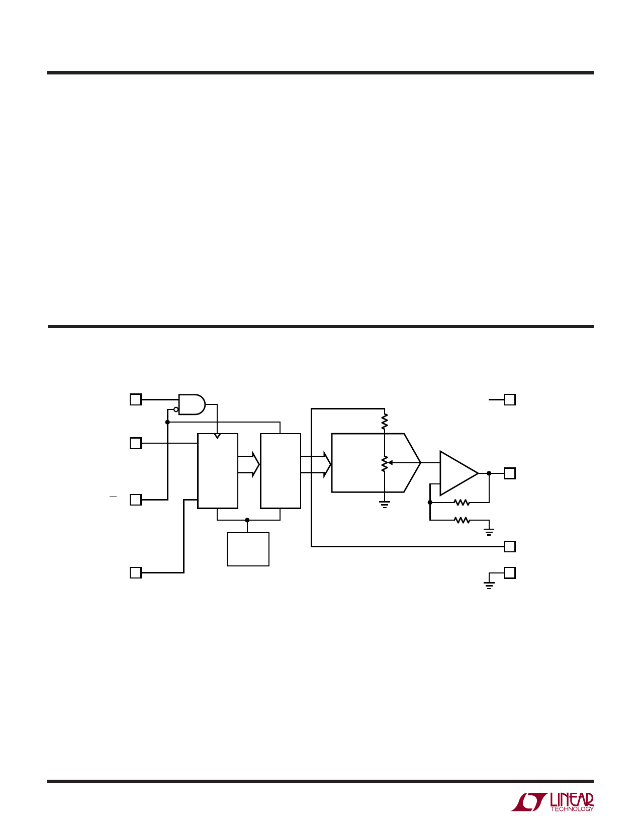
PIN FUNCTIONS
CLK (Pin 1): Serial Interface Clock. Internal Schmitt trigger
on this input allows direct optocoupler interface.
DIN (Pin 2): Serial Interface Data. Data on the DIN pin is
latched into the shift register on the rising edge of the
serial clock.
⎯C⎯S/LD (Pin 3): Serial Interface Enable and Load Control.
When ⎯C⎯S/LD is low the CLK signal is enabled, so the data
can be clocked in. When C⎯ S⎯ /LD is pulled high, data is loaded
from the shift register into the DAC register, updating the
DAC output and the CLK is disabled internally.
DOUT (Pin 4): Output of the Shift Register which Becomes
Valid on the Rising Edge of the Serial Clock.
GND (Pin 5): Ground.
REF (Pin 6): Reference Input. This pin can be tied to VCC.
The output will swing from 0V to REF. The typical input
resistance is 28k.
VOUT (Pin 7): Buffered DAC Output.
VCC (Pin 8): Positive Supply Input. 2.7V ≤ VCC ≤ 5.5V.
Requires a bypass capacitor to ground.
BLOCK DIAGRAM
CLK 1
DIN 2
CS/LD 3
DOUT 4
12-BIT
SHIFT
REGISTER
LD
DAC
REGISTER
POWER-ON
RESET
12-BIT
DAC
8 VCC
+
7 VOUT
–
6 REF
5 GND
1659 BD
1659fa
6
Share Link: 