CXA2598M Просмотр технического описания (PDF) - Sony Semiconductor
Номер в каталоге
Компоненты Описание
производитель
CXA2598M Datasheet PDF : 8 Pages
| |||
CXA2598M
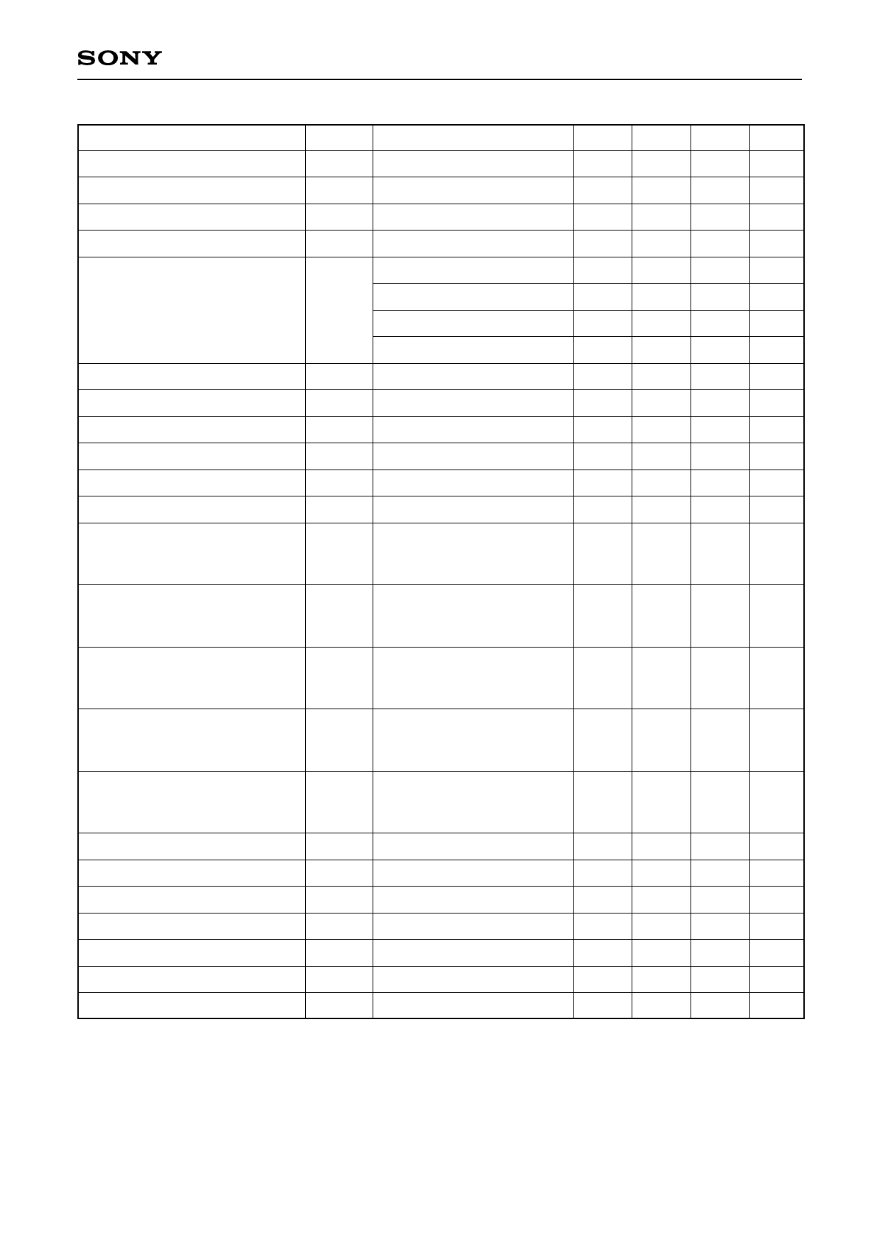
Electrical and Optical Characteristics
(VCC = 5.0V, VC = 2.5V, Ta = 25°C)
Item
Symbol
Conditions
Min. Typ. Max. Unit
Current consumption
ICC
In the dark
—
16
Output offset voltage (A to D) Voff
In the dark, Vc reference
–30
0
Output offset voltage (E to H) Voff
In the dark, Vc reference
–25
0
Output offset voltage (RF)
Voff
In the dark, Vc reference
–100
0
(A + B) – (C + D), in the dark –20
0
(A + D) – (B + C), in the dark –20
0
Output offset voltage difference ∆Voff
(A + C) – (B + D), in the dark –20
0
(E + G) – (F + H), in the dark –20
0
Offset temperature drift (A to H) ∆Voff/T In the dark
–100 —
Offset temperature drift (RF)
∆Voff/T In the dark
–1.0 —
Output voltage (A to D)
VO
λ = 780nm, Po = 10µW
82 110
Output voltage (E to H)
VO
λ = 780nm, Po = 10µW
338 450
Output voltage (RF)
Vo
λ = 780nm, Po = 10µW
165 220
Maximum output voltage (A to H, RF) VO
λ = 780nm, Po = 500µW
3.9 4.0
Frequency response 1 (A to D) fc
λ = 780nm
Po = 10µWDC, 4µWp-p
100kHz reference, –3dB
60 100
Frequency response 1 (E to H) fc
λ = 780nm
Po = 10µWDC, 4µWp-p
100kHz reference, –3dB
12
20
Frequency response 1 (RF)
fc
λ = 780nm
Po = 10µWDC, 4µWp-p
100kHz reference, –3dB
60 100
Frequency response 2 (A to D) ∆G
λ = 780nm
Po = 10µWDC, 4µWp-p
35MHz/100kHz
–0.5
0
λ = 780nm
Frequency response 2 (RF)
∆G
Po = 10µWDC, 4µWp-p
35MHz/100kHz
–1.0 0.5
Group delay difference (A to D) ∆Gd
100kHz to 35MHz
—
0.5
Group delay difference (RF)
∆Gd
100kHz to 35MHz
—
0.5
Settling time 1 (A to D)
Tset1 Output 500mV → 5mV
—
—
Settling time 1 (E to H)
Tset1 Output 500mV → 5mV
—
—
Settling time 2 (A to D)
Tset2 Output 500mV → 0.5mV
—
—
Slew rate (A to D)
SR
—
200
—
Slew rate (E to H)
SR
—
40
—
25 mA
30 mV
25 mV
100 mV
20 mV
20 mV
20 mV
20 mV
100 µV/°C
1.0 mV/°C
138 mV
563 mV
275 mV
—
V
— MHz
— MHz
— MHz
0.5 dB
1.0 dB
2
ns
2
ns
40
ns
70
ns
70
ns
— V/µs
— V/µs
Note 1) Output offset voltage: Vc is the reference.
Note 2) Output voltage: Vc is the reference. However, the offset voltage is excluded.
Note 3) Output voltage, offset temperature drift, frequency response, group delay difference, settling time,
slew rate: Confirmation of design.
Note 4) Measurement by the optical input: Measurement is made by emitting the light to the center of each
photodiode.
–2–
Share Link: 