MT88E39 Просмотр технического описания (PDF) - Mitel Networks
Номер в каталоге
Компоненты Описание
производитель
MT88E39 Datasheet PDF : 14 Pages
| |||
CMOS MT88E39
Calling Number Identification Circuit
Advance Information (CNIC1.1)
Features
• 1200 baud Bell 202 and CCITT V.23 Frequency
Shift Keying (FSK) demodulation
• Compatible with Bellcore GR-30-CORE,
SR-TSV-002476, TIA/EIA-716 and
ETSI 300 778-1
• High input sensitivity
• Dual mode 3-wire data interface (Serial FSK
data stream or MT88E43 compatible 1 byte
buffer)
• Internal gain adjustable amplifier
• Carrier detect status output
• Uses 3.579545 MHz crystal or ceramic
resonator
• 3 to 5V ±10% supply voltage
• Low power CMOS with power down mode
• Direct pin to pin replacement of MT8841 and
MT88E41
Applications
• Global (North America, Japan, Europe) FSK
based CID (Calling Identity Delivery) / CLIP
(Calling Line Identity Presentation)
• Feature phones, adjunct boxes
• FAX machines
• Telephone answering machines
• Computer Telephony Integration (CTI)
• Battery powered applications
DS5035
ISSUE 3
November 1998
Ordering Information
MT88E39AS 16 Pin SOIC
-40 to +85 °C
Description
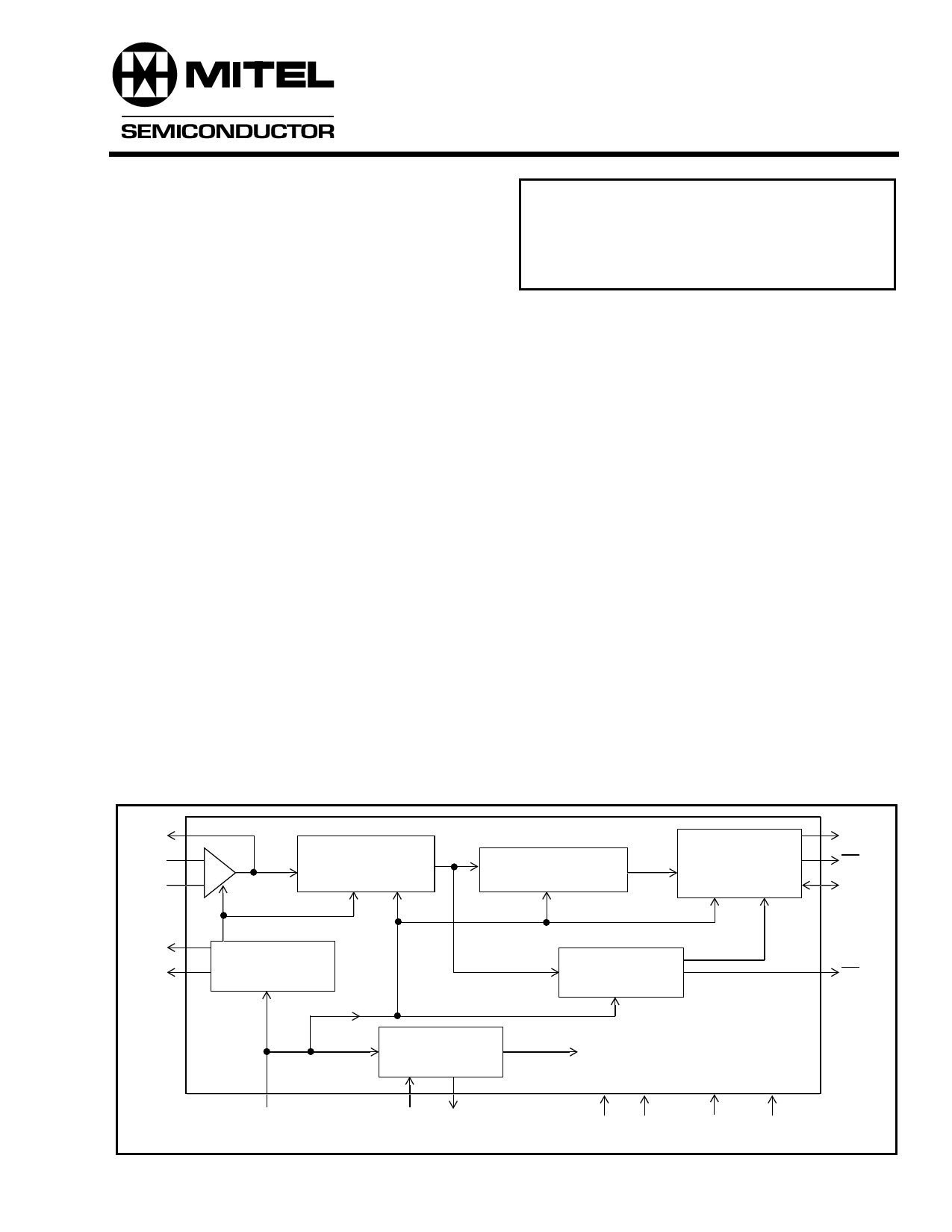
The MT88E39 Calling Number Identification Circuit
(CNIC1.1) is a CMOS integrated circuit which
provides an interface to calling line information
delivery services that utilize 1200 baud Bell 202 or
CCITT V.23 FSK data transmission schemes. The
MT88E39 receives and demodulates the FSK signal
and outputs the data into a simple dual mode 3-wire
serial interface which eliminates the need for an
UART.
The MT88E39 is Bellcore, ETSI and NTT compatible
and can operate in 3V and 5V applications. It is a pin
to pin replacement of the MT8841 and MT88E41 by
operating in the MT88E41 FSK interface mode
(mode 0) when placed in a MT88E41 socket. New
designs may also choose the MT88E43 compatible
interface (mode 1) where the microcontroller reads
the FSK byte from a 1 byte buffer.
GS
IN-
-
IN+
+
Receive
Bandpass
Filter
FSK
Demodulator
Data and Timing
Recovery
CAP
VRef
Bias
Generator
Carrier
Detector
Clock
Generator
to other
circuits
DATA
DR
DCLK
CD
PWDN
OSC1 OSC2
VSS VDD
MODE
IC
Figure 1 - Functional Block Diagram
5-1
Share Link: 