RF2362 Просмотр технического описания (PDF) - RF Micro Devices
Номер в каталоге
Компоненты Описание
производитель
RF2362 Datasheet PDF : 6 Pages
| |||
RF2362
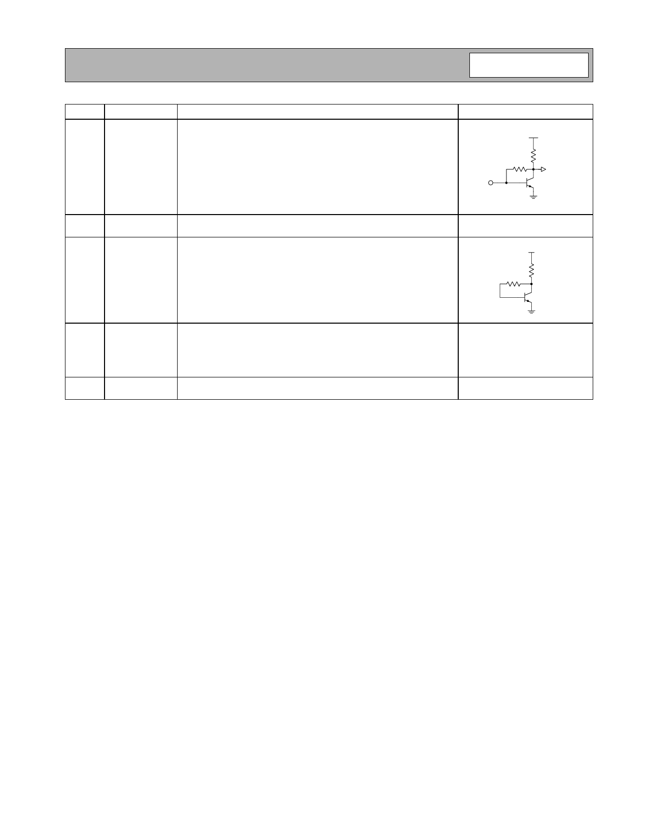
Pin Function Description
Interface Schematic
1
RF IN
RF input pin. This pin is DC-coupled and matched to 50Ω at 1880MHz.
PD
RF IN
2
GND1
Ground connection. For best performance, keep traces physically short
and connect immediately to ground plane.
3
VPD
Power Down for the IC. VPD = 2.8V +/- 0.1V turns on the part.
VPD<0.9V turns off the part. External RF bypassing is required. The
trace length between the pin and the bypass capacitors should be min-
imized. The ground side of the bypass capacitors should connect
immediately to ground plane. Nominal current required for VPD = 2.8V
is 8.5 mA typical and 12 mA Max (@VPD =2.9 V).
4
RF OUT Amplifier Output pin. This pin is an open-collector output. It must be
biased to either VCC or pin 4 through a choke or matching inductor.
This pin is typically matched to 50Ω with a shunt bias/matching induc-
tor and series blocking/matching capacitor. Refer to application sche-
matics.
5
GND2
Ground connection. For best performance, keep traces physically short
and connect immediately to ground plane.
TO OUTPUT
STAGE
PD
Rev A5 020607
4-343
Share Link: 