SP8855E Просмотр технического описания (PDF) - Mitel Networks
Номер в каталоге
Компоненты Описание
производитель
SP8855E Datasheet PDF : 14 Pages
| |||
SP8855E
A minimum value for the pull down resistor is 330 Ohms. When
the Fpd and Fref outputs are disabled the output level will be at
the logic low level of about 3.5V so that the additional supply
current due to the load resistors will be present even when the
outputs are disabled.
Reference input
The reference input circuit functions as an input amplifier or
crystal oscillator. When an external reference signal is used
this is simply AC coupled to pin 28, the base of the input
emitter follower. When a low phase noise synthesiser is
required the reference signal is critical since any noise present
here will be multiplied by the loop. To obtain the lowest
possible phase noise from the SP8855E it is best to use the
highest possible reference input frequency and to divide this
down internally to obtain the required frequency at the phase
detector. The amplitude of the reference input is also
important, and a level close to the maximum will give the
lowest noise. When the use of a low reference input frequency
say 4-10MHz is essential some advantage may be gained by
using a limiting amplifier such as a CMOS gate to square up
the reference input.
In cases where a suitable reference signal is not available,
it may be more convenient to use the input buffer as a crystal
oscillator in this case the emitter follower input transistor is
connected as a Colpitts oscillator with the crystal connected
from the base to ground and with the feedback necessary for
oscillation provided by a capacitor tap at the emitter. The
arrangement is shown inset in Fig. 5.
C1
C2
FROM
CHARGE
PUMP
OUTPUT
FROM
CHARGE
PUMP
REFERENCE
R2
-
TO
+
VCO
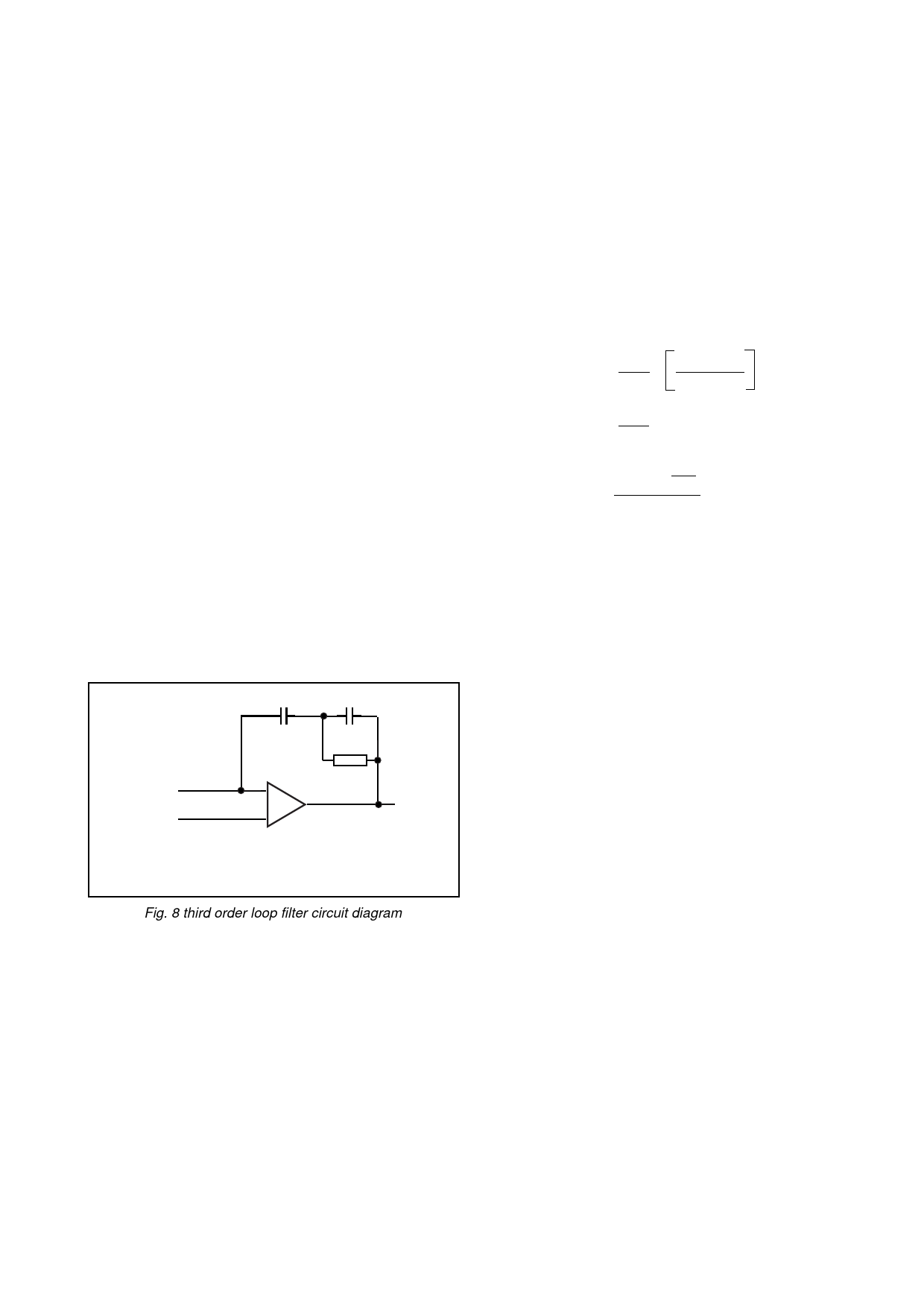
Fig. 8 third order loop filter circuit diagram
Loop Filter Design
Generally the third order filter configuration shown in Fig.8
gives better results than the more commonly used second
order because the reference sidebands are reduced. Three
equations are required to determine values for the three
constants where;
τ1 = C1
τ2 = R2 (C1 + C2)
τ3 = C2 R2
The equations are
1
τ1
=
Kφ K0
Nωn2
1 + ωn2 τ22 1/2
1 + ωn2 τ32
2
τ2 =
1
ωn2 τ3
3
τ3 =
-
tan
φο
+
1
cos
φο
ωn
Where;
Kφ is the phase detector gain factor in mA/radian
K0 is theVCO gain factor in radian/second/Volt
N is the total division ratio from VCO to reference
frequency
ωn is the natural loop bandwidth
φο is the phase margin normally set to 45°
Since the phase detector is linear over a range of 2π radian,
Kφ can be calculated from
Kφ = Phase comparator current setting/2π mA/radian
These values can now be substituted in equation 1 to obtain
a value for C1 and equation 2 and 3 used to determine values
for C2 and R2
EXAMPLE
Calculate values for a loop with the following parameters
Frequency to be synthesised:
Reference frequency
Division ratio
ωn natural loop frequency
K0 VCO gain factor
φ0 phase margin
Phase comparator current
1000MHz
10MHz
1000MHz/10MHz = 100
100KHz
2π x 10MHz/Volt
45°
6.3mA
The phase detector gain factor Kφ
= 6.3mA /2π = 1mA/radian
11
Share Link: 