HT27C512 –ü—Ä–ĺ—Ā–ľ–ĺ—ā—Ä —ā–Ķ—Ö–Ĺ–ł—á–Ķ—Ā–ļ–ĺ–≥–ĺ –ĺ–Ņ–ł—Ā–į–Ĺ–ł—Ź (PDF) - Holtek Semiconductor
–Ě–ĺ–ľ–Ķ—Ä –≤ –ļ–į—ā–į–Ľ–ĺ–≥–Ķ
–ö–ĺ–ľ–Ņ–ĺ–Ĺ–Ķ–Ĺ—ā—č –ě–Ņ–ł—Ā–į–Ĺ–ł–Ķ
–Ņ—Ä–ĺ–ł–∑–≤–ĺ–ī–ł—ā–Ķ–Ľ—Ć
HT27C512 Datasheet PDF : 10 Pages
| |||
HT27C512
Absolute Maximum Ratings
Operation Temperature Commercial ...................................................................................0¬įC to +70¬įC
Storage Temperature......................................................................................................... ‚Äď65¬įC to 125¬įC
Applied VCC Voltage with Respect to VSS ........................................................................ ‚Äď0.6V to 7.0V
Applied Voltage on Input Pin with Respect to VSS........................................................... ‚Äď0.6V to 7.0V
Applied Voltage on Output Pin with Respect to VSS............................................... ‚Äď0.6V to VCC+0.5V
Applied Voltage on A9 Pin with Respect to VSS.............................................................. ‚Äď0.6V to 13.5V
Applied VPP Voltage with Respect to VSS .......................................................................‚Äď0.6V to 13.5V
Applied READ Voltage (Functionality is guaranteed between these limits) ................ +4.5V to +5.5V
Note: These are stress ratings only. Stresses exceeding the range specified under “Absolute Maxi-
mum Ratings‚ÄĚ may cause substantial damage to the device. Functional operation of this device
at other conditions beyond those listed in the specification is not implied and prolonged
exposure to extreme conditions may affect device reliability.
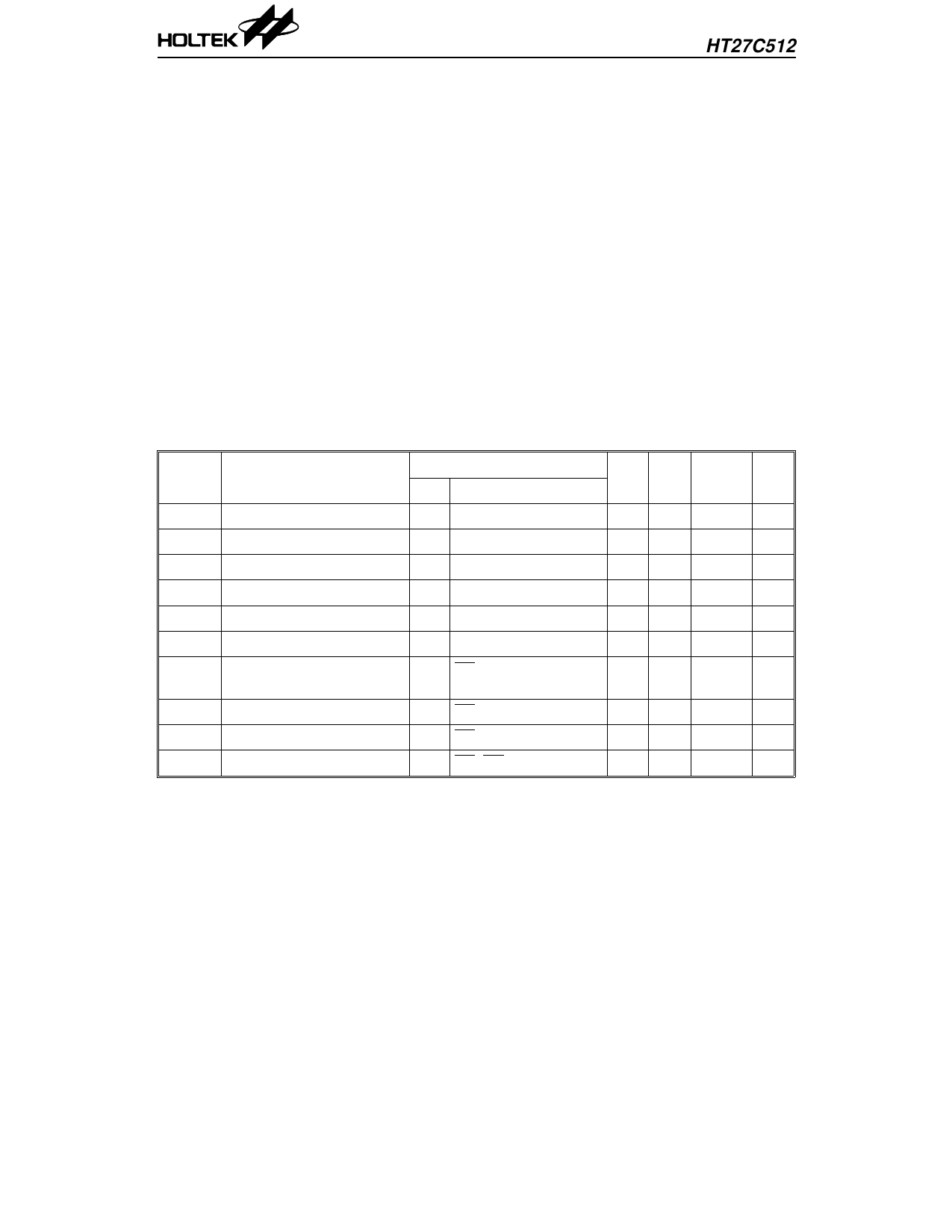
D.C. Characteristics
Read operation
Symbol
Parameter
Test Conditions
VCC
Conditions
Min. Typ. Max. Unit
VOH Output High Level
5V IOH=‚Äď0.4mA
2.4 ‚ÄĒ
‚ÄĒ
V
VOL Output Low Level
5V IOL=2.1mA
‚ÄĒ ‚ÄĒ 0.45 V
VIH Input High Level
5V
‚ÄĒ
2.0 ‚ÄĒ VCC+0.5 V
VIL
Input Low Level
5V
‚ÄĒ
‚Äď0.3 ‚ÄĒ
0.8
V
ILI
Input Leakage Current
5V VIN=0 to 5.5V
‚Äď5 ‚ÄĒ
5
¬ĶA
ILO
Output Leakage Current
5V VOUT=0 to 5.5V
‚Äď10 ‚ÄĒ
10
¬ĶA
ICC
VCC Active Current
5V
CE=VIL, f=5MHz,
IOUT=0mA
‚ÄĒ‚ÄĒ
30 mA
ISB1 Standby Current (CMOS) 5V CE=VCC¬Ī0.3V
‚ÄĒ 1.0 10 ¬ĶA
ISB2 Standby Current (TTL)
5V CE=VIH
‚ÄĒ ‚ÄĒ 1.0 mA
IPP
VPP Read/Standby Current 5V CE=OE=VIL, VPP=VCC ‚ÄĒ ‚ÄĒ
100 ¬ĶA
3
6th May ’99
Share Link: 