SP8852EIGHCAR –ü—Ä–æ—Å–º–æ—Ç—Ä —Ç–µ—Ö–Ω–∏—á–µ—Å–∫–æ–≥–æ –æ–ø–∏—Å–∞–Ω–∏—è (PDF) - Mitel Networks
–ù–æ–º–µ—Ä –≤ –∫–∞—Ç–∞–ª–æ–≥–µ
–ö–æ–º–ø–æ–Ω–µ–Ω—Ç—ã –û–ø–∏—Å–∞–Ω–∏–µ
–ø—Ä–æ–∏–∑–≤–æ–¥–∏—Ç–µ–ª—å
SP8852EIGHCAR Datasheet PDF : 13 Pages
| |||
the charge pump outputs when high. During this period the
VCO control voltage will be maintained by the loop filter
components around the loop amplifier, but due to the com-
bined effects of the amplifier input current and charge pump
leakage a gradual change will occur. In order to reduce the
change, the duration of the strobe pulse should be minimised.
Selection of a loop amplifier with low input current will reduce
the VCO voltage droop during the strobe pulse and result in
minimum reference sidebands from the synthesiser.
Reference Input
The reference source can be either driven from an external
sine or square wave source of up to 100MHz or a crystal can
be connected as shown in Fig. 5.
Phase Comparator and Charge Pump
The SP8852E has a digital phase/frequency comparator
driving a charge pump with programmable current output.
The charge pump current level at the minimum gain setting is
approximately equal to the current fed into the RSET input, pin
19, and can be increased by programming the bus according
to Table 2 by up to 4 times.
Bit 15 Bit 14
Current multiplication factor
0
0
1·0
0
1
1·5
1
0
2·5
1
1
4·0
Table 2
Pin
19
current
=
VCC21·6V
RSET
Phase
detector
gain
=
IPIN19
(mA)3multiplication
2p
factor
mA/rad
To allow for control direction changes introduced by the
design of the PLL, bit 12 on the input bus address 0 can be
programmed to reverse the sense of the phase detector by
transposing the FPD and FREF connections. In order that any
external phase detector will also be reversed by this program-
ming bit, the FPD and FREF outputs are also interchanged by
bit 12 as shown in Table 3.
SP8852E
Output for RF phase lag
Sense bit (bit 12)
Pin 20
1
Current source
0
Current sink
Table 3
The FPD and FREF signals to the phase detector are
available on pins 24 and 25 and may be used to monitor the
frequency input to the phase detector or used in conjunction
with an external phase detector. These outputs may be
programmed by bits 10 and 11 of word 0 according to Table 4.
State 3, where the outputs are disabled by the lock detect
circuit, is useful where the user wishes to use an external
phase detector. The internal phase/frequency detector may
be used to pull the loop into lock and an automatic switch-over
to the external phase detector made. When the FPD and FREF
outputs are to be used at high frequencies, an external pull
down resistor of minimum value 330Ω may be connected to
ground to reduce the fall time of the output pulse.
Bit 11 Bit 10
Phase detector state
0
0 Enabled, FPD and FREF off
0
1 Enabled, FPD and FREF on
1
0 Disabled by lock detect, FPD and FREF on
1
1 Disabled, FPD and FREF on
Table 4
The charge pump connections to the loop amplifier consist
of the charge pump output and the charge pump reference.
The matching of the charge pump up and down currents will
only be maintained if the charge pump output is held at a
voltage equal to the charge pump reference using an
operational amplifier to produce a virtual earth condition at pin
20. The lock detect circuit can drive an LED to give visual
indication of phase lock or provide an indication to the control
system if a pullup resistor is used in place of the LED. A small
capacitor connected form the C-LOCK DETECTOR pin to
ground may be used to delay lock detect indication and
remove glitches produced by momentary phase coincidence
during lock up.
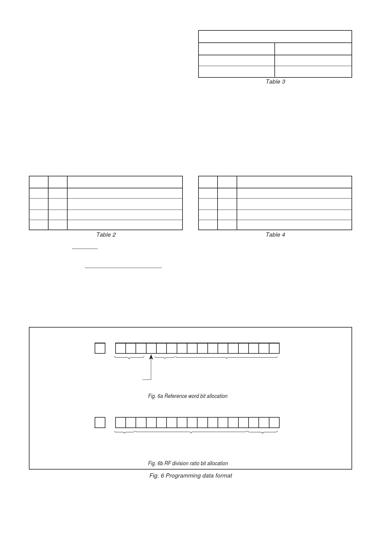
PIN 40
BIT 15
PIN 11
BIT 0
0
29 28 27 26 25 24 23 22 21 20
ADDRESS
NOT USED
PHASE
DETECTOR
SENSE
CONTROL
(SEE TABLE 3)
PHASE
DETECTOR
STATE
CONTROL
(SEE TABLE 4)
10-BIT REFERENCE COUNTER
Fig. 6a Reference word bit allocation
PIN 40
BIT 15
PIN 11
BIT 0
1
213 212 211 210 29 28 27 26 25 24 23 22 21 20
ADDRESS
PHASE
DETECTOR
GAIN
CONTROL
(SEE TABLE 2)
M COUNTER
Fig. 6b RF division ratio bit allocation
3-BIT
A COUNTER
Fig. 6 Programming data format
7
Share Link: 