LC74730M Просмотр технического описания (PDF) - SANYO -> Panasonic
Номер в каталоге
Компоненты Описание
производитель
LC74730M Datasheet PDF : 14 Pages
| |||
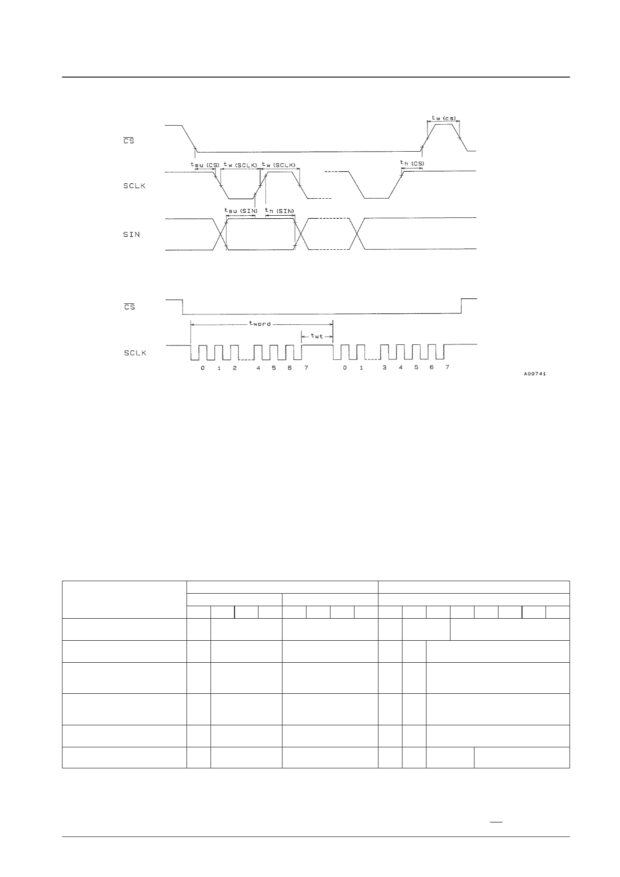
Serial Data Input Timing
LC74730M
Display Control Commands
The display control commands have an 8-bit serial input format. Commands consist of a first byte, which includes the
command identification code, and data in the second and following bytes. The LC74730M supports the following
commands:
x COMMAND 0: Display memory (VRAM) write address setup command
y COMMAND 1: Display character data write command
z COMMAND 2: Vertical display start position and vertical size setup command
{ COMMAND 3: Horizontal display start position and horizontal size setup command
| COMMAND 4: Display control setup command
} COMMAND 5: Synchronizing signal control setup command
Display Control Command Table
First byte
Command
Command identification code
Data
7
6
5
4
3
2
1
0
7
COMMAND 0
Set write address
1
0
0
0 V3 V2 V1 V0 0
COMMAND 1
Write character
1
0
0
1
0
0
0
0
at
COMMAND 2
Set vertical display start position and 1
0
1
0 VS VS VS VS 0
vertical character size
21 20 11 10
COMMAND 3
Set horizontal display start position
1
0
1
1 HS HS HS HS 0
and horizontal character size
21 20 11 10
COMMAND 4
Display control
1
1
0
0 TST CB OSC SYS 0
MOD
STP RST
COMMAND 5
Synchronizing signal control
1
1
0
1 PH PH BCL INT 0
1
0
Second byte
Data
6
5
4
3
2
1
0
0
0 H4 H3 H2 H1 H0
0 c5 c4 c3 c2 c1 c0
0 VP VP VP VP VP VP
5
4
3
2
1
0
0 HP HP HP HP HP HP
5
4
3
2
1
0
0 NON EG BK BK RV DSP
1
0
ON
0
0
0 SN SN SN SN
3
2
1
0
The command identification code in a first byte is retained until the next first byte is written. However, if a display
character data write command (COMMAND 1) is written, the LC74730M locks in display character data write mode,
and the first byte cannot be overwritten.
The command state is reset to the COMMAND 0 state (display memory address setup mode) when the CS pin is set high.
No. 4247-5/14
Share Link: 